5ECC0 Electronics II
- Area: Electronics
- Topics: Transfer Functions and Frequency Response · Transistor Amplifiers · Operational Amplifiers · Oscillators and Waveform Generators · Data Converters · Digital Logic
- Related courses: Electronics I - 5ECB0 · Biopotential and Neural Interface Circuits - 5XCC0 · Computation II - 5EIB0
- Resit notes: Current Mirror (resit) - 5ECC0 · Data Converter (resit) - 5ECC0 · Differential Amplifier (resit) - 5ECC0 · MOSFET (resit) - 5ECC0 · Op-Amp (resit) - 5ECC0 · Oscillator Circuit (resit) - 5ECC0 · Overview (resit) - 5ECC0
Content
Lab, 1 Assigment, 2 Homeworks, 2 Lecture Quizzes
Formula Sheet Given
Background knowledge (given by Georgi Radulov)
o Network theory, poles and zeros
o Electronics (transistor circuits), MOSFET
o Small signal and Large signal analysis, biasing
o Mathematics (differentiate, integrate, complex numbers)
Signal generators and waveform-shaping circuits (given by Georgi Radulov)
o sine-wave oscillators
o limiting and clamping
o op-amp RC oscillator circuits
o LC and Xtal oscillator
Frequency response (given by Georgi Radulov)
o frequency dependency
o multi-stage amplifier frequency response
Integrated-circuit amplifiers (given by Georgi Radulov)
o finite open-loop gain and bandwidth
o large-signal operation
o cmos transistor level design and analysis
Operational amplifier circuits (given by Georgi Radulov)
o two-stage CMOS op-amp characteristic properties
o Miller compensation
o Output stages
o CMOS class AB output stages
Data converters (given by Pieter Harpe)
o digital-to-analog converters
	▪ Op-amp based
	▪ R2R ladder
	▪ Charge redistribution
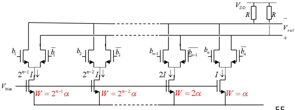
	▪ Current-steering
o analog-to-digital converters
	▪ flash
	▪ tracking
	▪ SAR
	▪ Dual-slope
CMOS digital logic circuits (given by Eugenio Cantatore)
o digital logic inverters
o CMOS inverter
o dynamic operation of CMOS inverter
o CMOS logic-gate circuits
o CMOS transmission gates
Memory circuits (given by Eugenio Cantatore)
o latches and flip-flops
o static and dynamic memories
o sense amplifiers
o read-only memories
Background knowledge
General
-
, we convert it to imaginary so we don’t use derivatives:
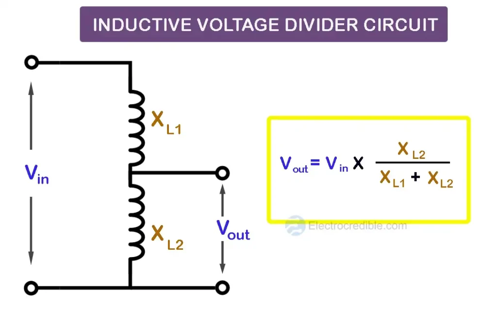
Impedance (resistance, reactance):
V,I type:where
, , amplitude
Capacitors (Ohms law):
,
Inductors (Ohms law):, charge in capacitor:
-
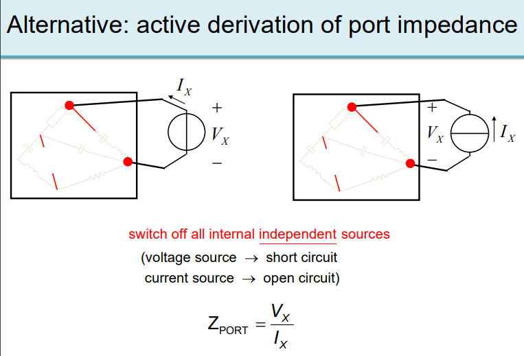
voltage source: short circuit, current source: open circuit
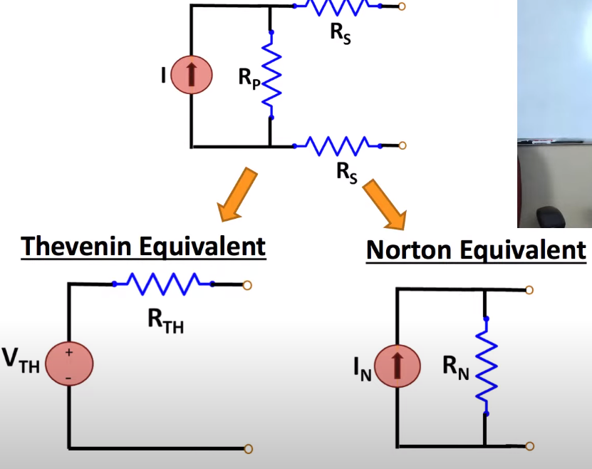
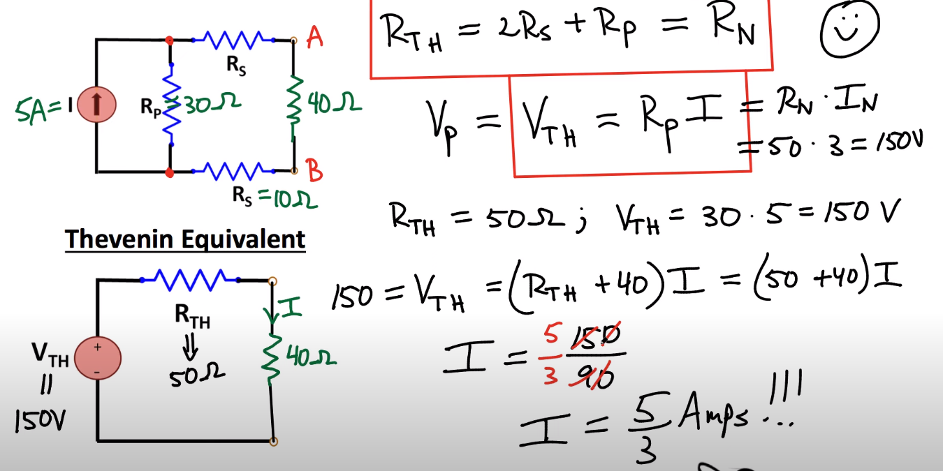
Thevenin/Norton: https://www.youtube.com/watch?app=desktop&v=h9rA42B1euw
Impedance (opamps):and
gyrator:
Admittance:
Electronics I - 5ECB0 > Op-Amps
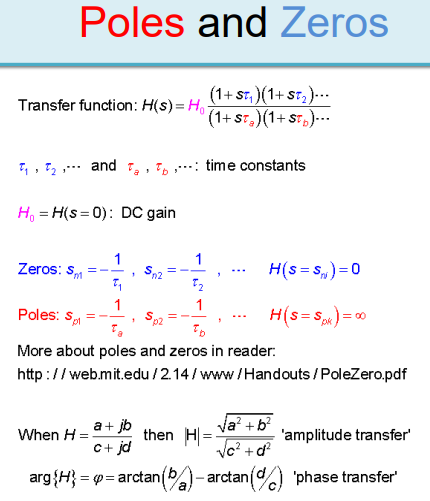
Poles Zeros
Poles & Zeros: https://www.youtube.com/watch?v=AZ7_MvANy_Q
Systems - 5ESB0
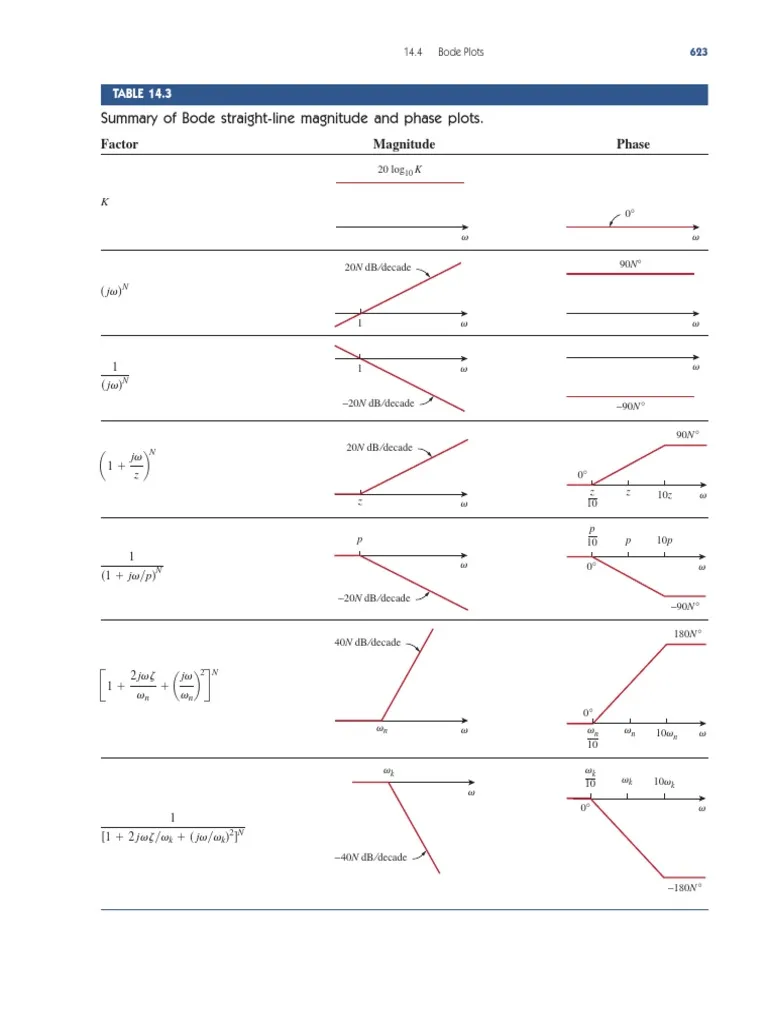
Gain (dB) =
Phase =
Analysis
Electronics I - 5ECB0 > Diodes
large signal → bias point → tangent → initialization → small signal
Small Signal Analysis:
I source = OC
V source = SC
Capacitors = SC
Inductance = OC
V bias = ground
Bias analysis:
V source = SC
Capacitors = OC
MOSFET
small signal: https://www.youtube.com/watch?v=utBRWK4GmmE
active-load: https://www.youtube.com/watch?v=IOCK41RNpGs
cs: https://www.youtube.com/watch?v=T-0X1N9N5V8&t=363s
cg: https://www.youtube.com/watch?v=2zr5ykXpyXY
cascode: https://www.youtube.com/watch?v=uFxXgDCLhGw
mirror: https://www.youtube.com/watch?v=Jmu02dErhdg
differential-1: https://www.youtube.com/watch?v=IYR-FxjAym0&t=5s
differential-2: https://www.youtube.com/watch?v=nWz6JGyT_fo
Electronics I - 5ECB0 > MOSFET/MOST
MOSFET Visuals: https://www.youtube.com/watch?v=rkbjHNEKcRw
MOSFET Logic: https://www.youtube.com/watch?v=g3kn4yeAjEI
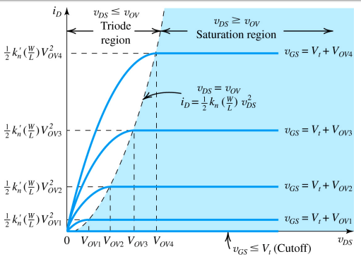
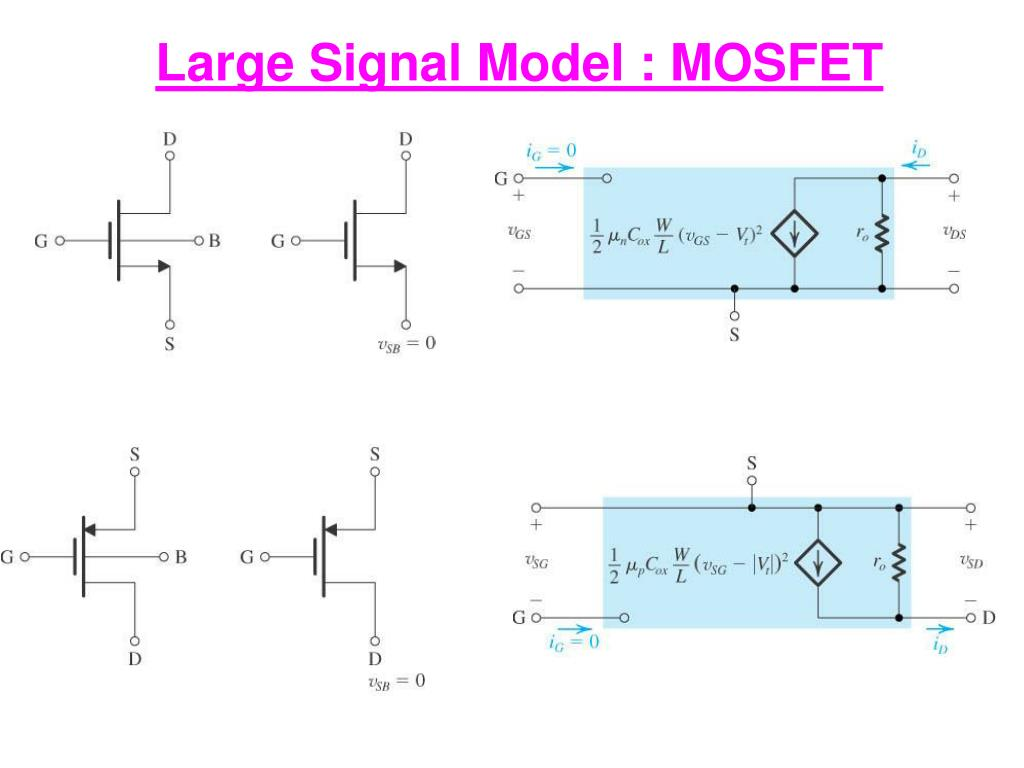
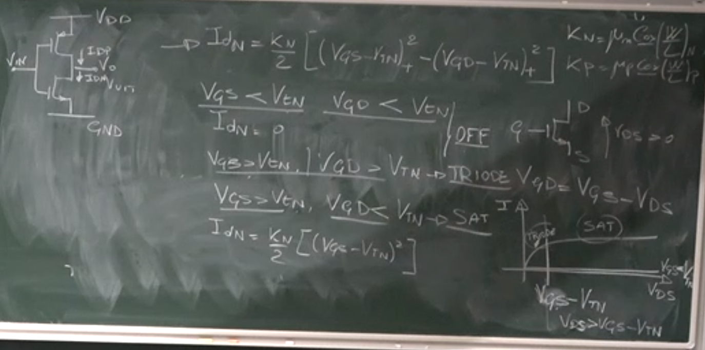
- MOSFET Drain Currents:
- NMOS Satured if:
so if → V controlled I source - PMOS Saturated if:
so if - When saturated:
- When triode:
Modes
triode:
and
saturated:and
cut-off:and
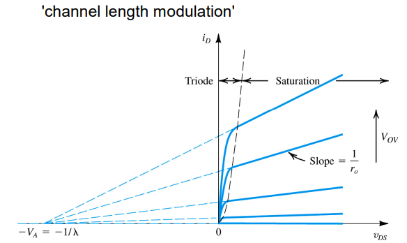
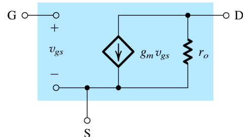
Small signal equivalent of MOSFETs
(saturation)
(saturation)
if body effect:
transistors act as voltage (
) controlled current ( ) sources
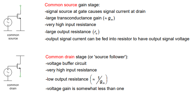
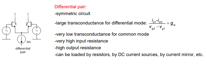
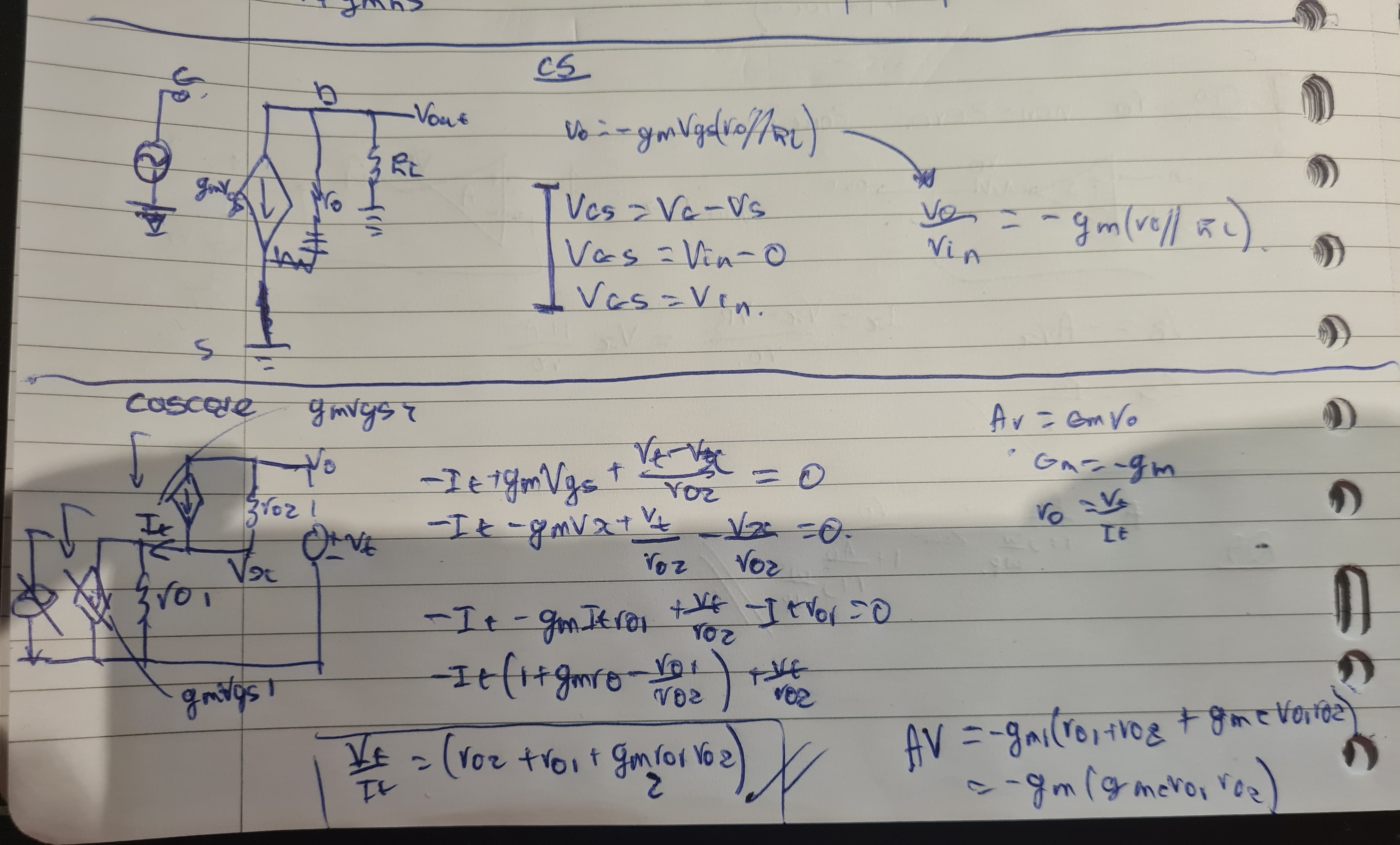
common-source
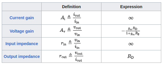
common-drain
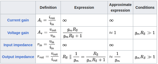
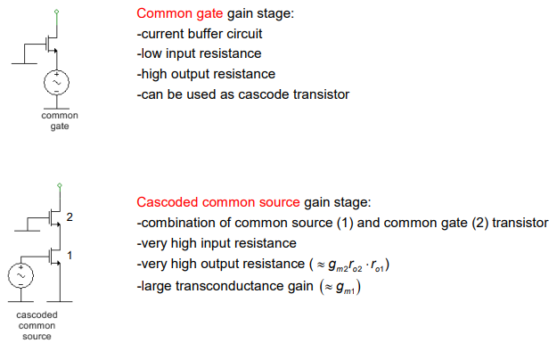
common-gate
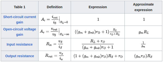
cascode
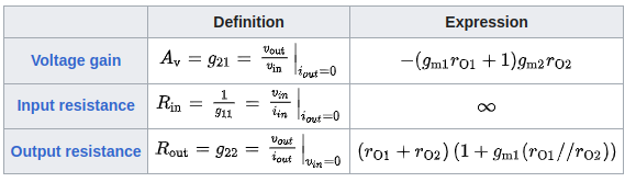
if all equal
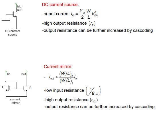
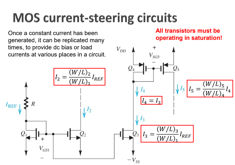
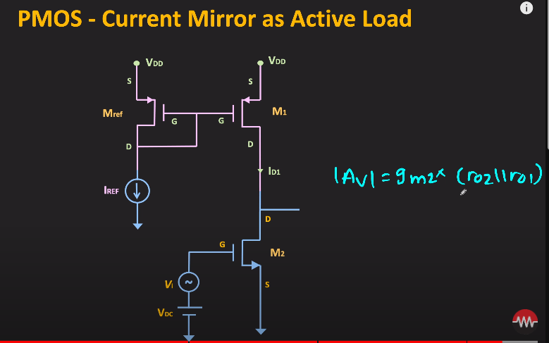
current-mirror
Signal generators and waveform-shaping circuits
Topic: Oscillators and Waveform Generators
oscillator: https://www.youtube.com/watch?v=XVS8Puf4tiw
there are: RC, LC, Crystal oscillators
Sine-Wave Oscillators
Oscillator Feedback Loop:
open-loop gain:
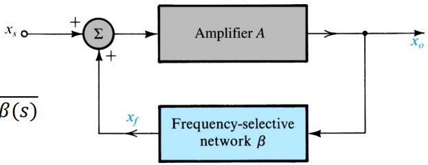
Barkhausen criteria: At the oscillation frequency,
- the phase of the open loop gain should be
(“right moment”, no phase shift in signal) → - and the magnitude should be
(“right amount”, no gain no decrease in amplitude) →
Op-Amp RC Oscillators
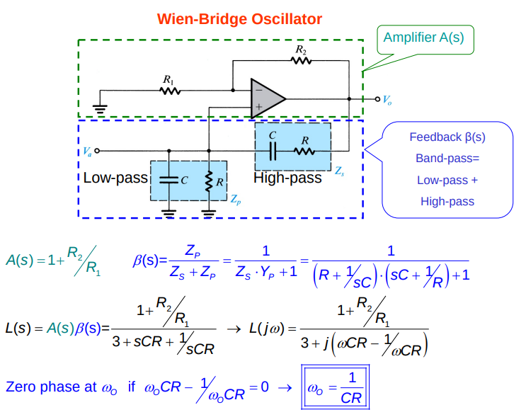
Wien-Bridge Oscillator
https://www.youtube.com/watch?v=gbUXbaxvX94
Zero phase at
at
Formulas
Oscillations at stable amplitude
for for for
~=slightly
Small amplitude ⇒ Open-loop gain == >~1
Large amplitude ⇒ Open-loop gain == <~1 → (as soft clipping comes on)
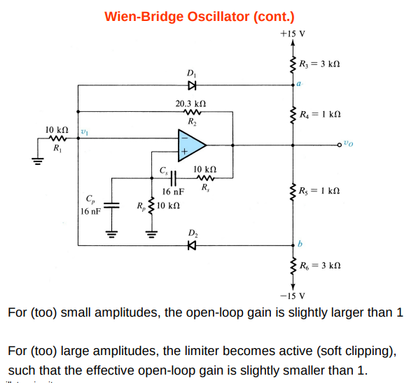
wien bridge with a limiter
Formulas
top diode: min amplitude, bottom diode: max amplitude peak
then you can findmeaning after amplitude reaches that voltage one of diodes turn on
First the oscillations start where
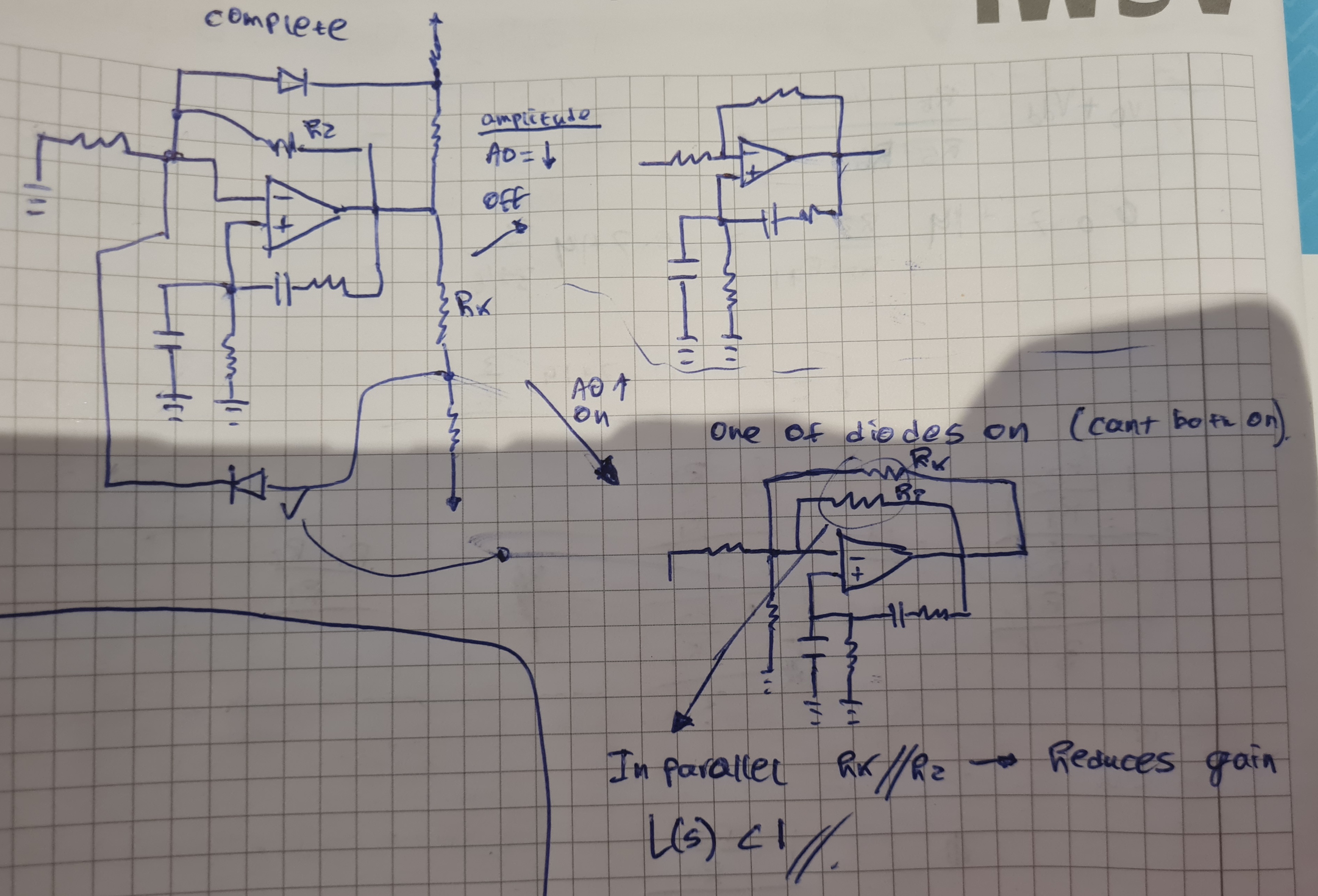
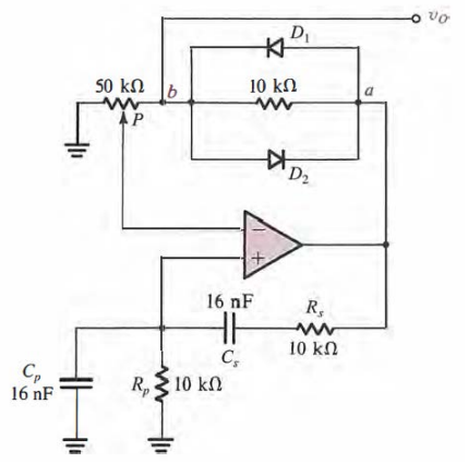
Amplitude (voltage divider between a and (b=o)):
[!NOTE] (Passive) Limiter Circuits
amplitude dependent gain
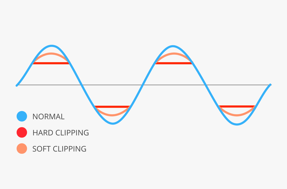
Hard Limiter (clipper): higher amplitude → higher attenuation → distortion
Soft Limiter: less distortion:
- (ideal diode),
- (ideal diode with voltage source (0.7V))
- (ideal diode with voltage source and resistor)
- exponential model:
where at
limiters: Electronics I - 5ECB0 > Summary for EC2
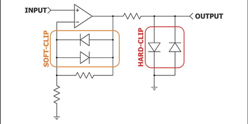
Soft Clipping gets clipped in the feedback loop of an op amp.
Hard Clipping gets clipped after the feedback loop.
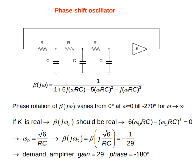
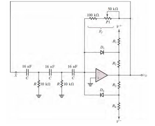
Phase Shift Oscillator
https://www.youtube.com/watch?app=desktop&v=Gvb4GIV5ig8
If
→
→ demand amplifier
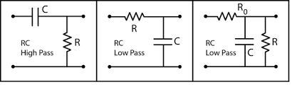
take voltage divider: high-pass:
each pass filter is
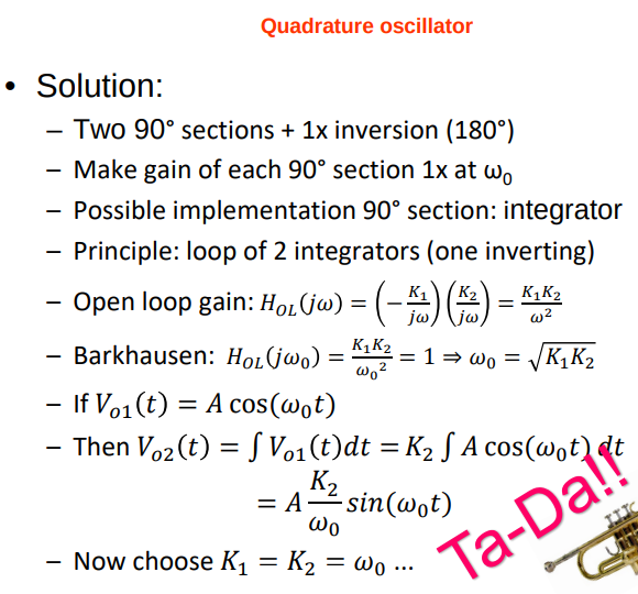
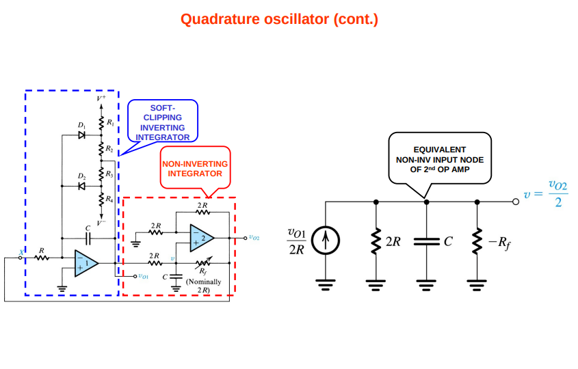
Quadrature Oscillator
circuit integrator: https://www.youtube.com/watch?v=OPvs7A554Rw
LC and Crystal Oscillators
LC Oscillators
intuition: https://youtu.be/2_y_3_3V-so?si=gklbMfbzDkME4z3v
colpitts: https://www.youtube.com/watch?v=1fgw-ONlAcc
lc-tuned: https://www.youtube.com/watch?v=u-B9YRWMtpQ
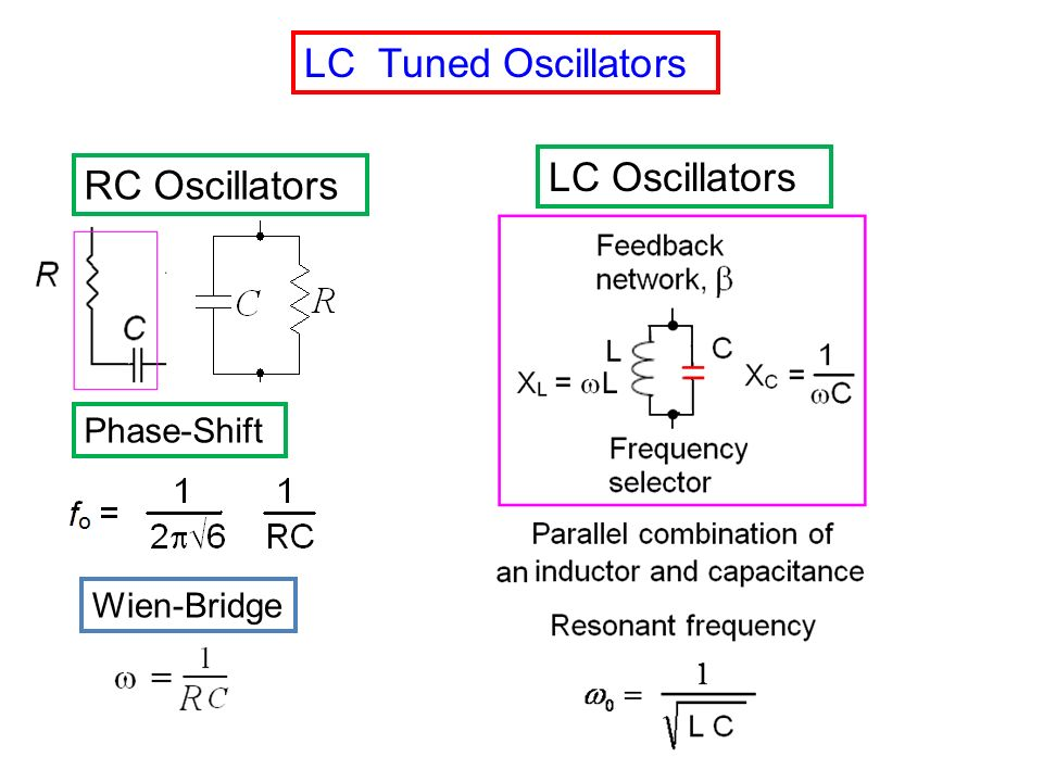
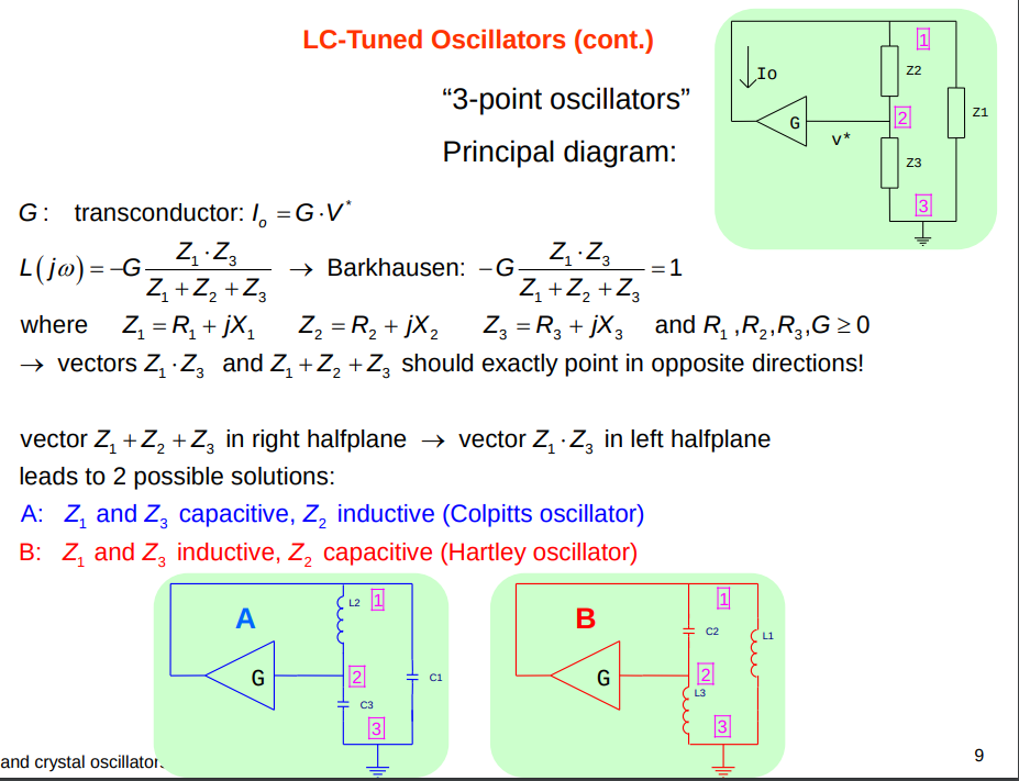
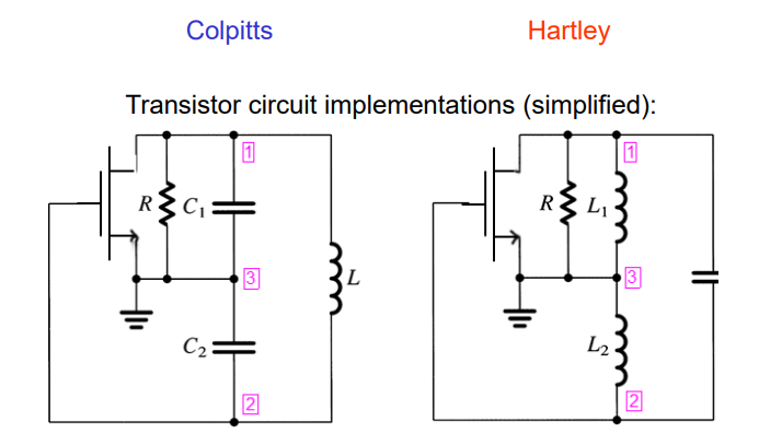
we need the amplifier so that the oscillations don’t die out (watch video for colpitts)
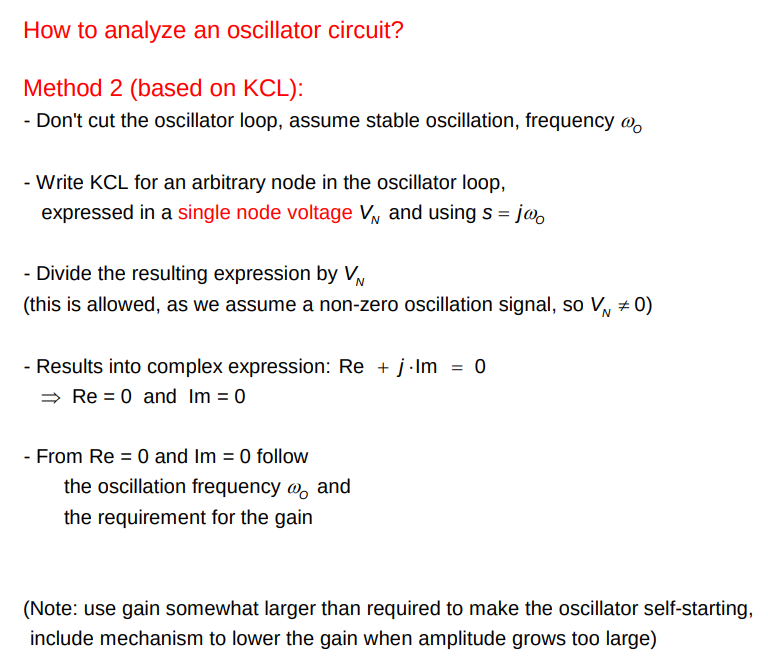
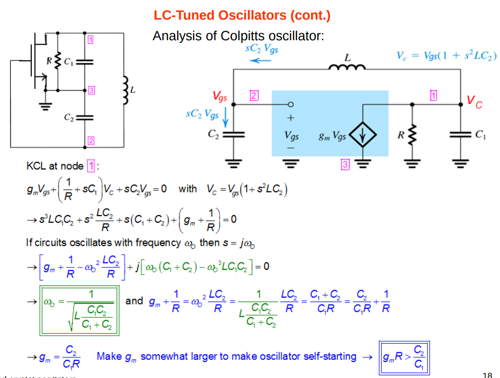
Colpitts Oscillator:
Hartley Oscillator:
Crystal Oscillators
summary: https://www.youtube.com/watch?v=YzcKQWwkzWs
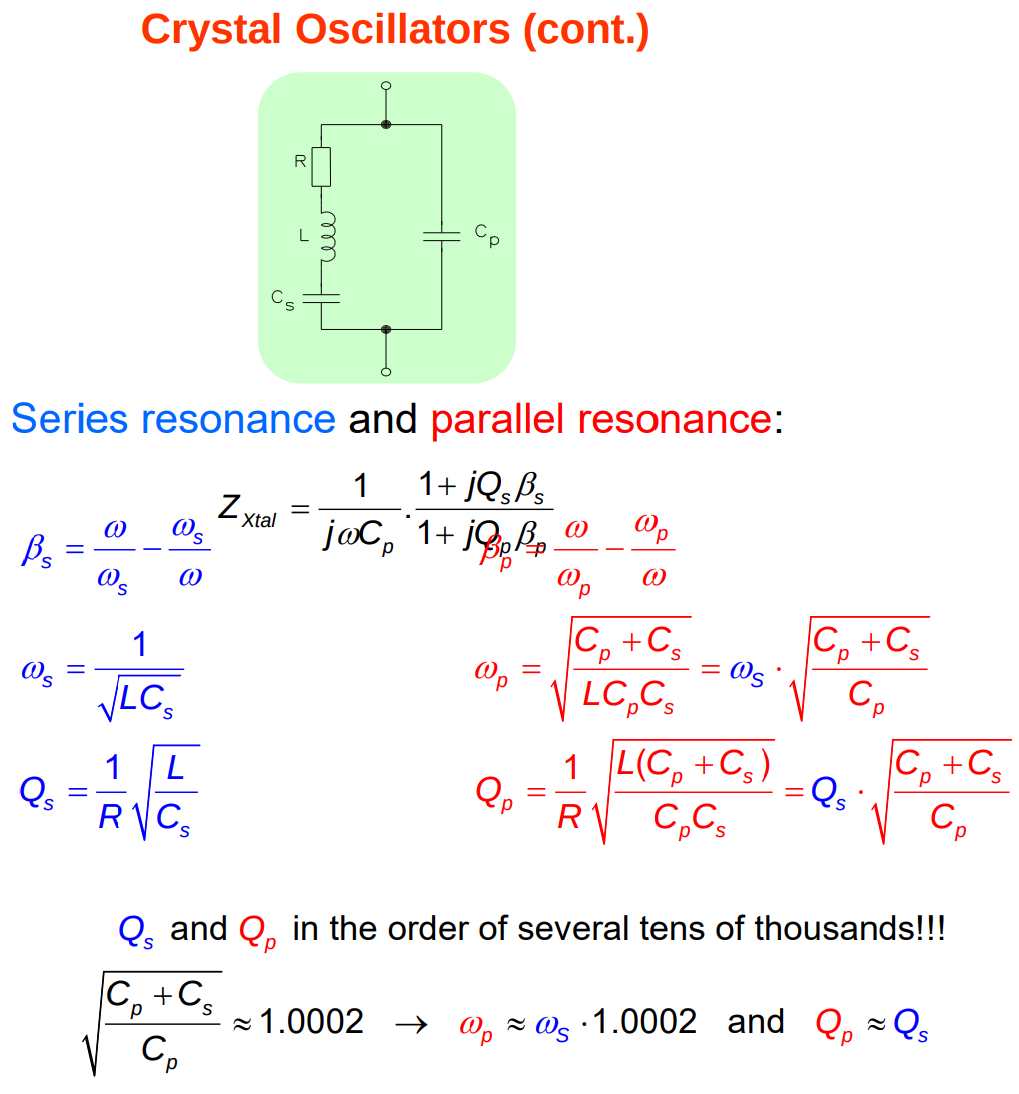
capacitive (no DC current possible)
series resonance: resistive, low ohmic, determined by crystal properties
inductive: phase corrections→small shifts
parallel resonance: resistive, high ohmic, slightly influenced by
capacitive
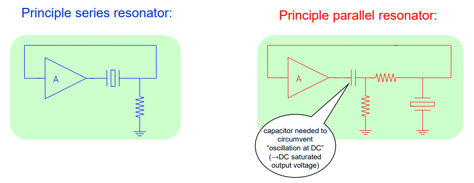
series:
parallel:
parallel:
Frequency response
Topic: Transfer Functions and Frequency Response
Amplifier Circuits
Frequency Dependence
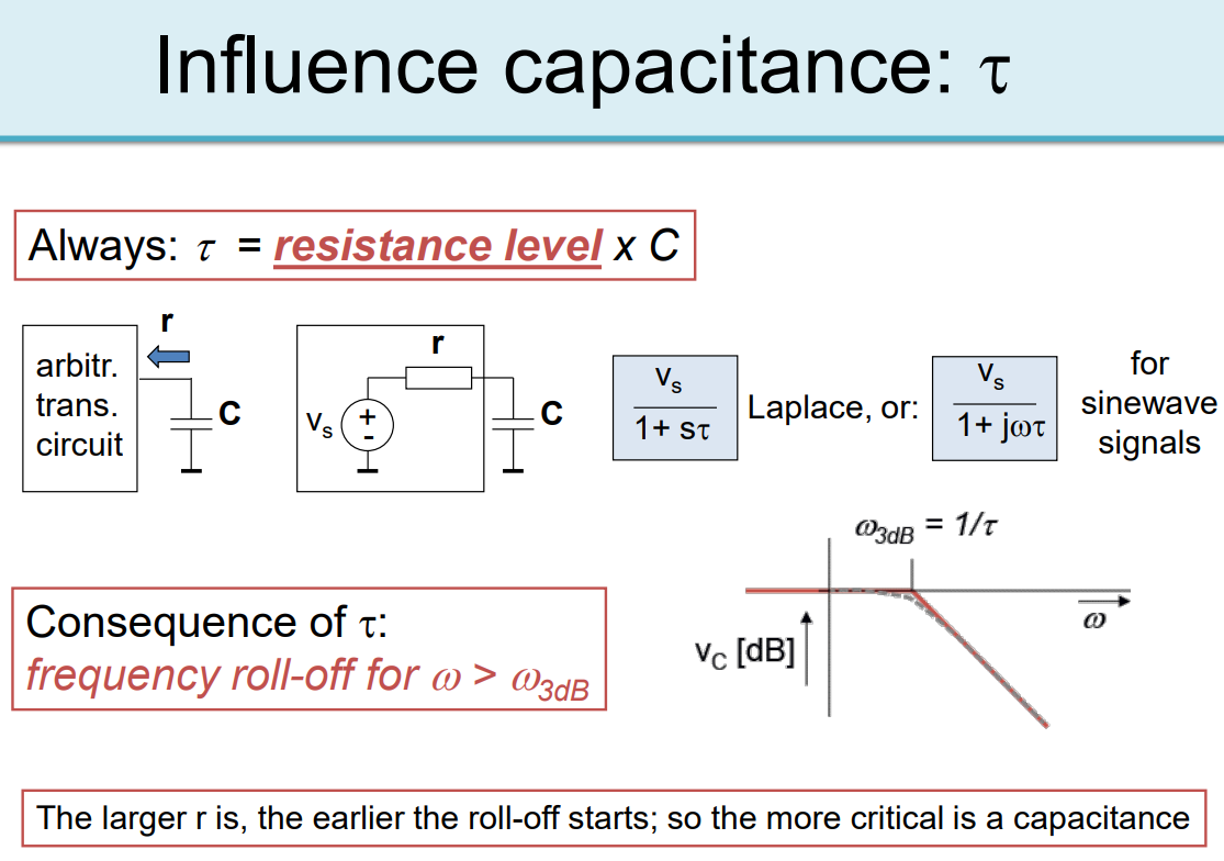
It is an important value because it signifies the circuit’s growth rate or decay. The lower the value of the time constant of a circuit, the higher the rate of growth or decay of the circuit. And the higher the value of the time constant of a circuit, the lower the rate of growth or decay.
decay: discharge of capacitance
→ settle to a constant voltage after time, poll frequency
everything after →
long time constants = long setting
short time constants = quick settings
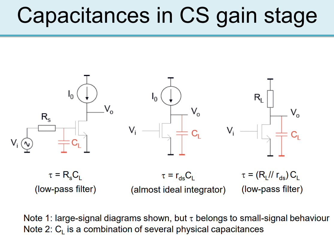
Capacitance in CS gain stage
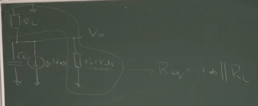
CS Amplifier
phase rotation:
input resistance:
gain at high: low
gain at low: high
so effect of time constant so higher as this signal passes through that time constant (single pole, low pass filter) → the higher frequencies the more attenuation we will have. So the gain will reduce as it passes through this low pass filter. that’s why gain at low : high attenuation → reduction in signal strength
one pole adds attenuation and phase shift
Capacitances in CG gain stage
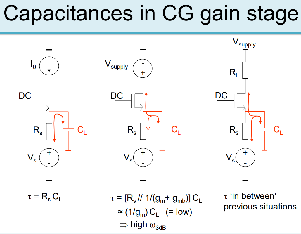
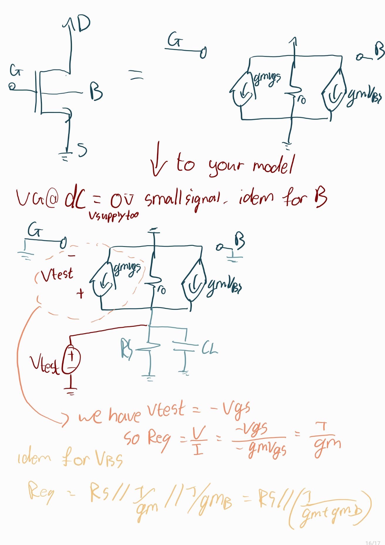
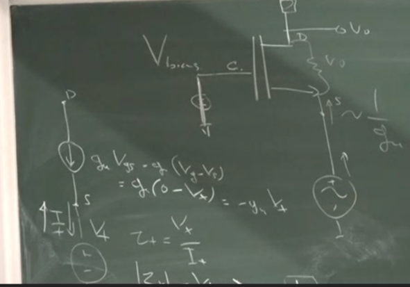
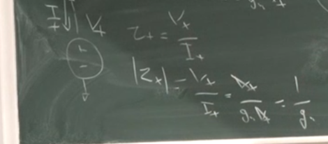
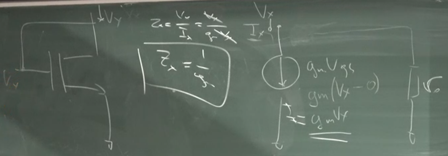
if we considered
Capacitance in Current Mirrors
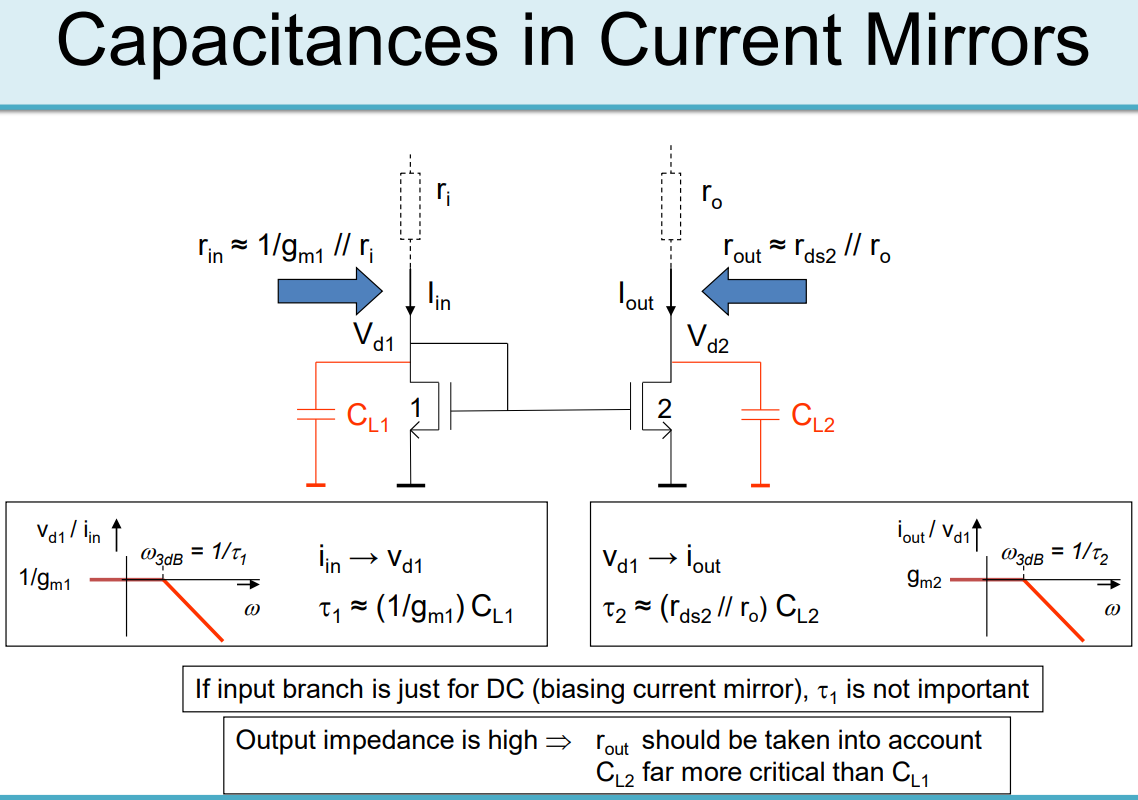
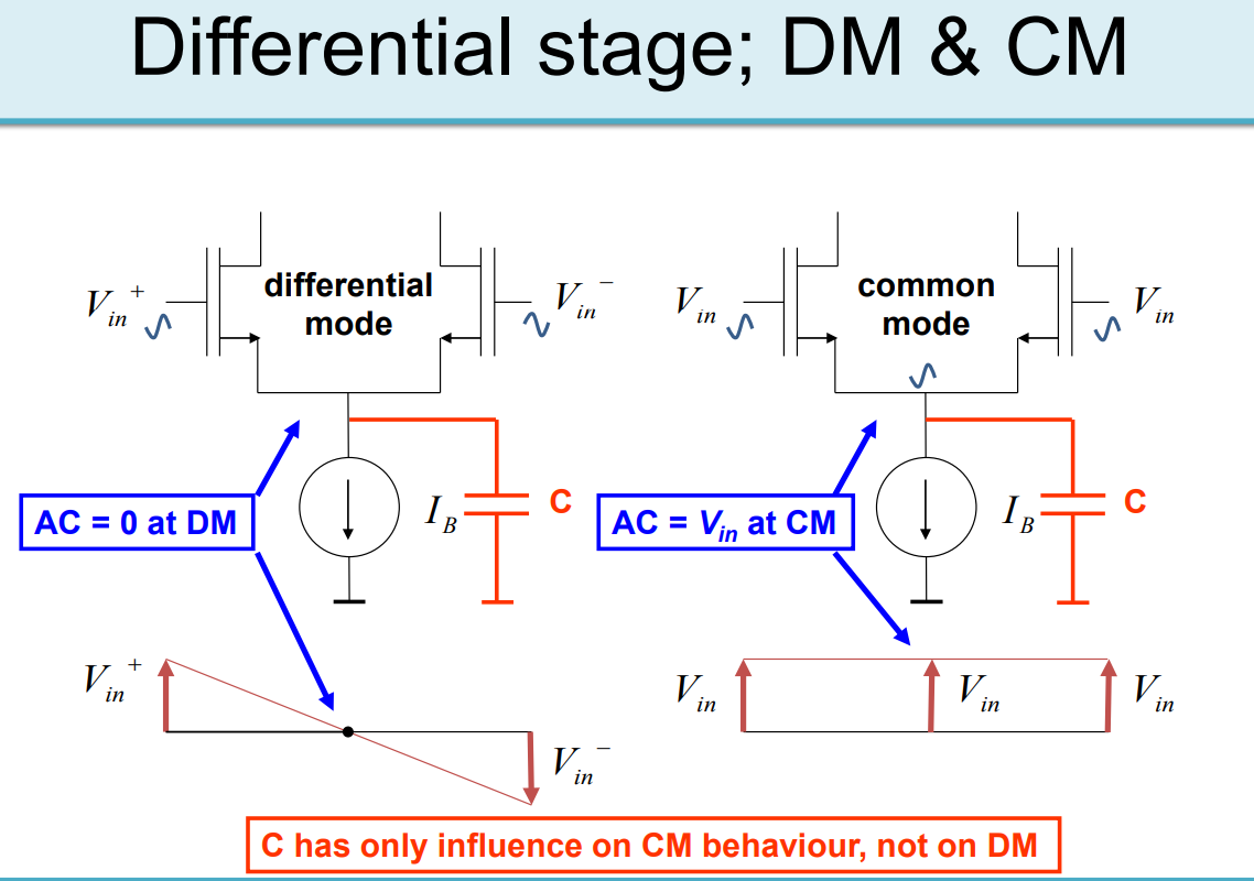
in DM both signals are affected as
in CM
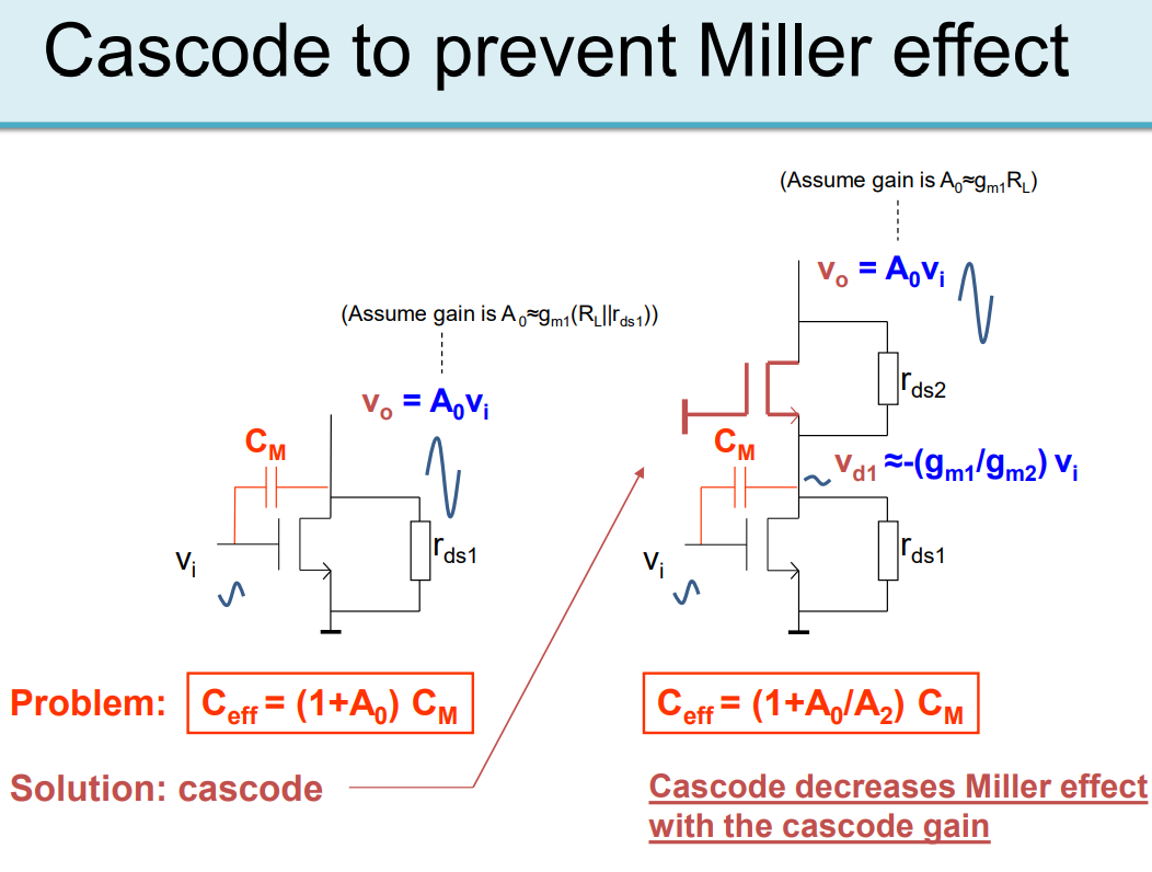
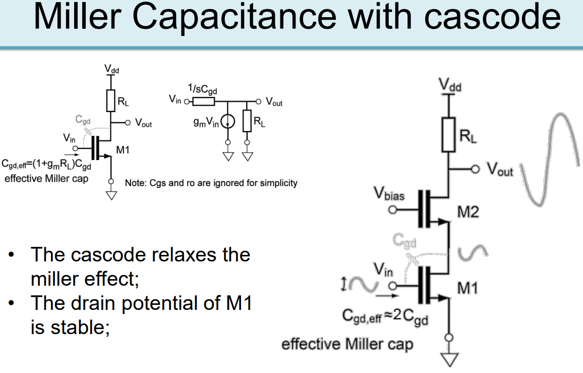
Miller capacitances
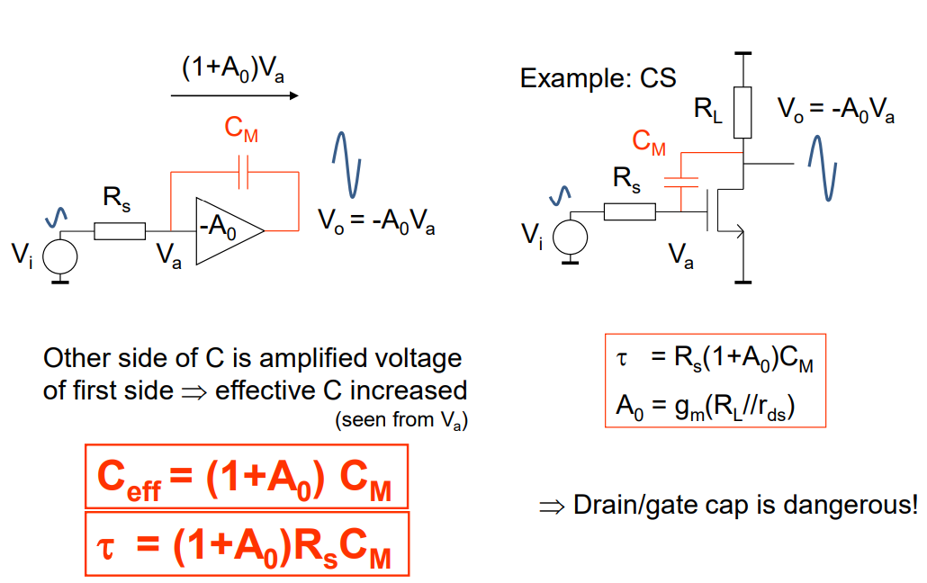
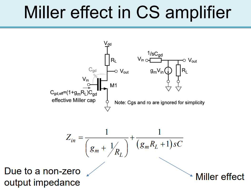
In electronics, the Miller effect accounts for the increase in the equivalent input capacitance of an inverting voltage amplifier due to amplification of the effect of capacitance between the input and output terminals. The virtually increased input capacitance due to the Miller effect is given by:
.
Effect in CS amplifier
cascode amplifier miller: https://www.youtube.com/watch?v=Op_I3Ke7px0
 1
Integrated-circuit amplifiers
Topic: Transistor Amplifiers
Finite Open-Loop Gain and Bandwidth on Circuit Performance
gain bandwidth: https://www.youtube.com/watch?v=wfkzz1rg-xk
gain bandwidth product: https://en.wikipedia.org/wiki/Gain%E2%80%93bandwidth_product
slew rate: https://www.youtube.com/watch?v=2DFIr6t1hbc
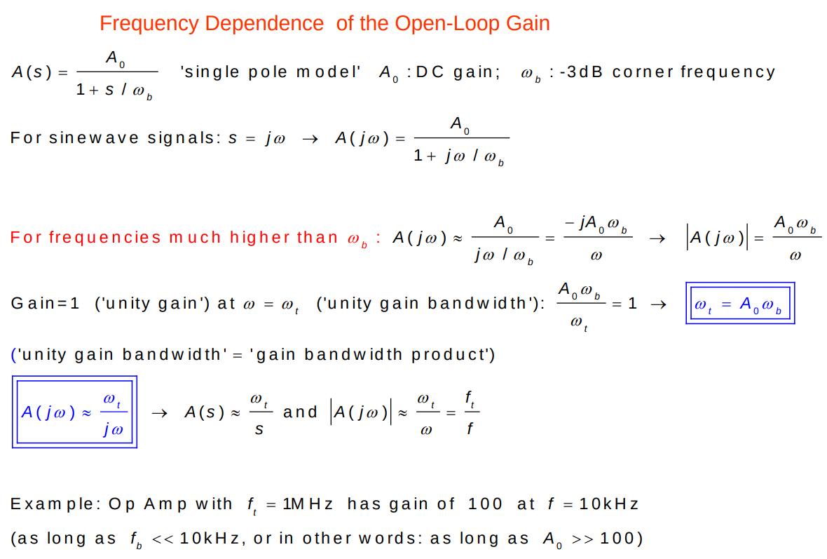
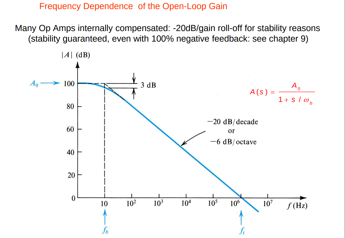
cascading put a gain to the power of cascades, 3 cascades → to power 3.
open loop gain→
For an inverting/non-inverting amplifier
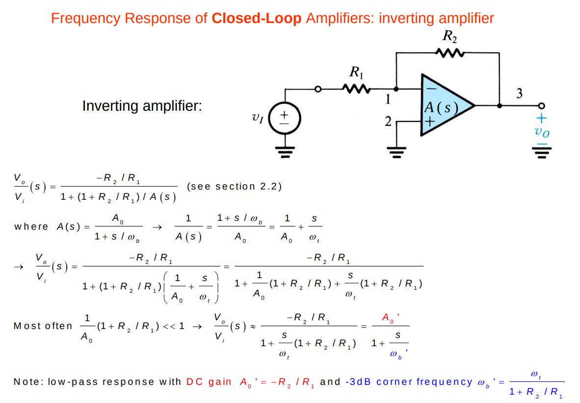
→
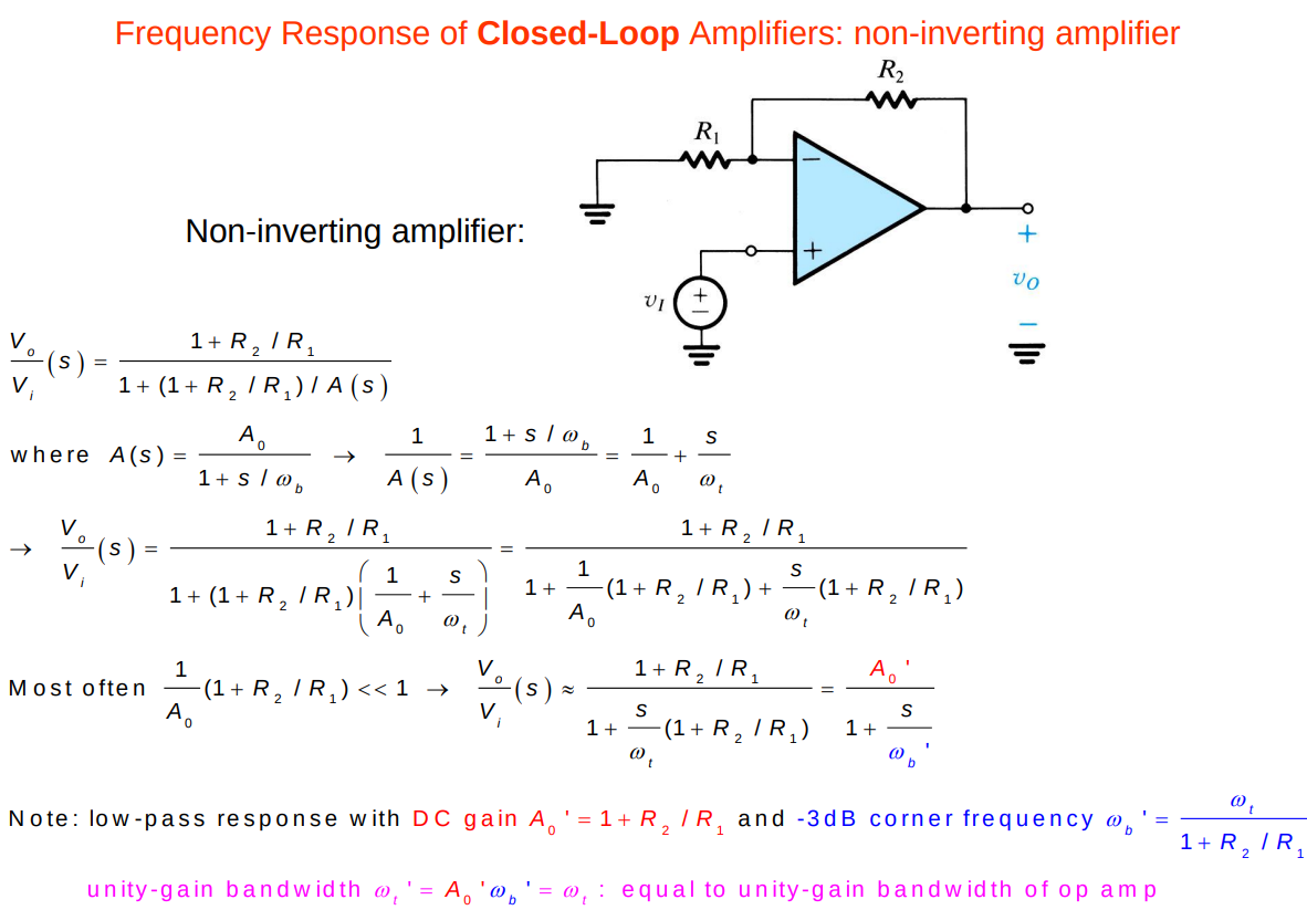
inverting:
Large – Signal Operation of Op Amps
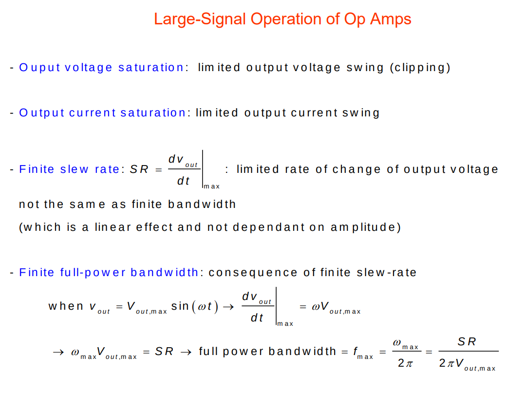
clipping: imagine a non inverting amplifier with a gain of 10, and if you provide
Operational amplifier circuits
Topic: Operational Amplifiers
current mirror ota: https://www.youtube.com/watch?v=Gzpn_oywnf4
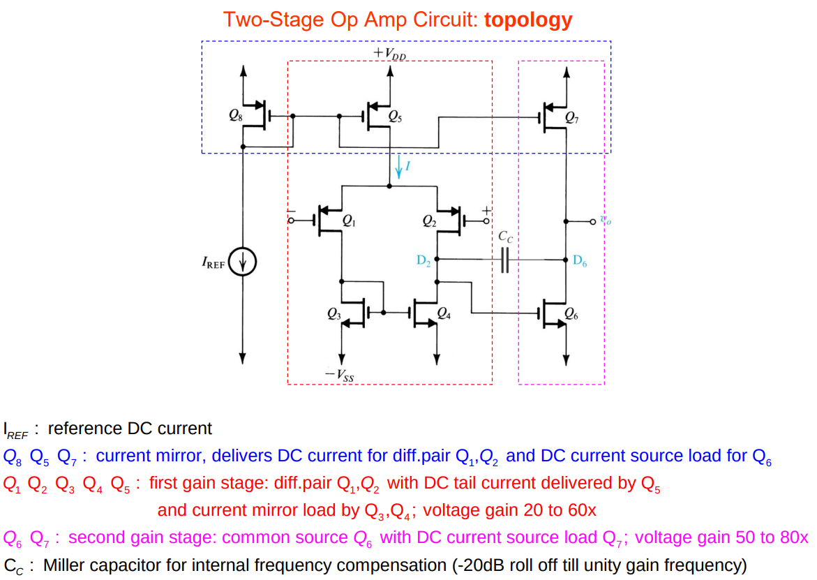
Frequency response of a Two-Stage CMOS Op Amp
Transistor Config: Electronics I - 5ECB0 > Summary for EC2
- no small signal component in the the first part of the schematic so small signal ground, explained in lecture, since as different signal changes, one side increases current and the other lowers.
- stage is completed when:
conversions happen at 2 stages of the schematic
https://videocollege.tue.nl/mediasite/Showcase/11d4c5f4423c453ba67db38aef7ba22744/Presentation/8ab31336825f4736b934bcd9949e4c121d
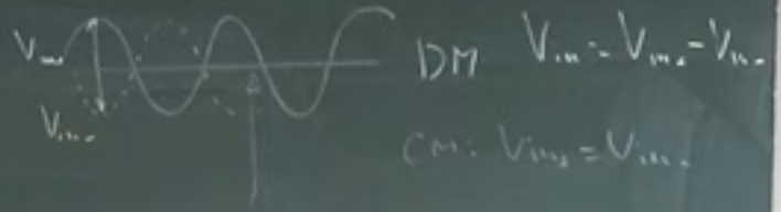
we reject common mode since if there is a disturbance the common signal is affected while differential doesn’t so we amplify it with amplifier. splits in 2 → due to current mirror - increasing
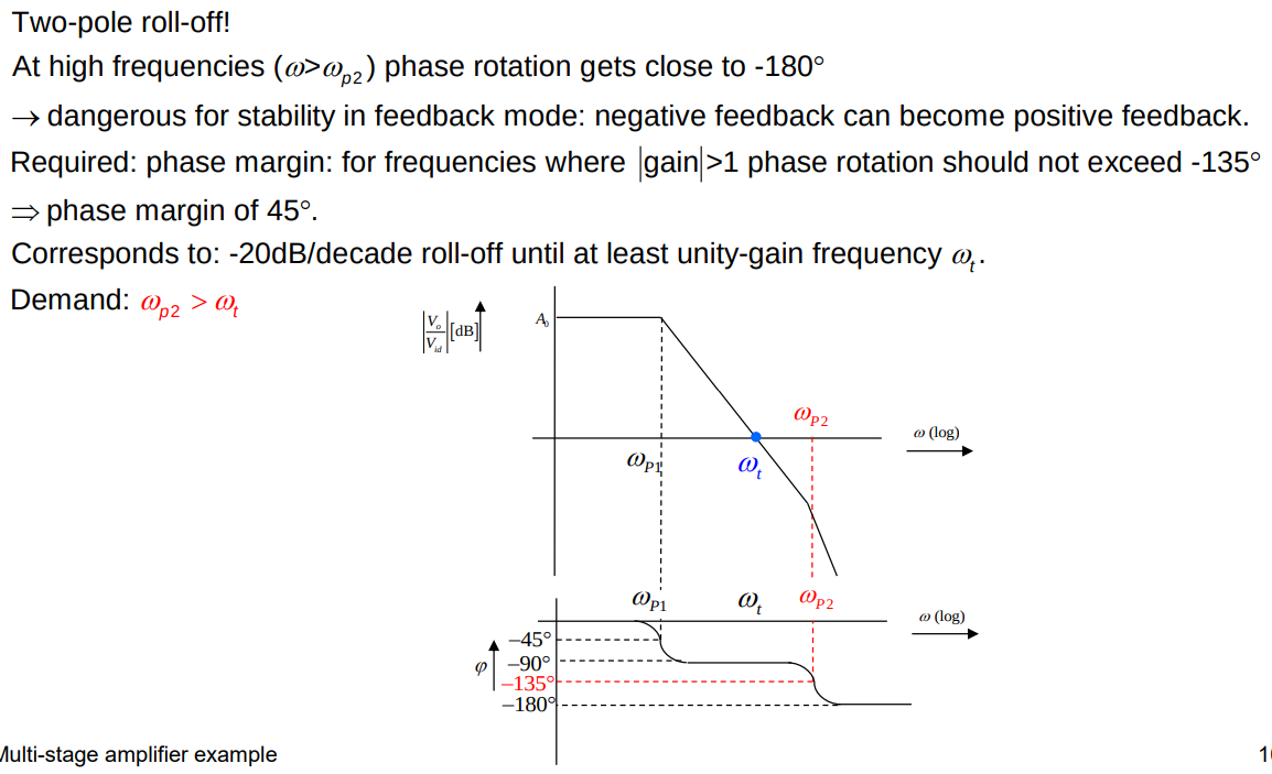
and on the other side vice versa decrease and is the bias current and then we modulate it - **for stable amplifier the between
and total phase rotation must be lower than phase margin, or else we get an oscillator… - **
1 pole

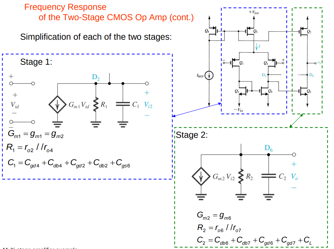
Stage 1
Stage 2
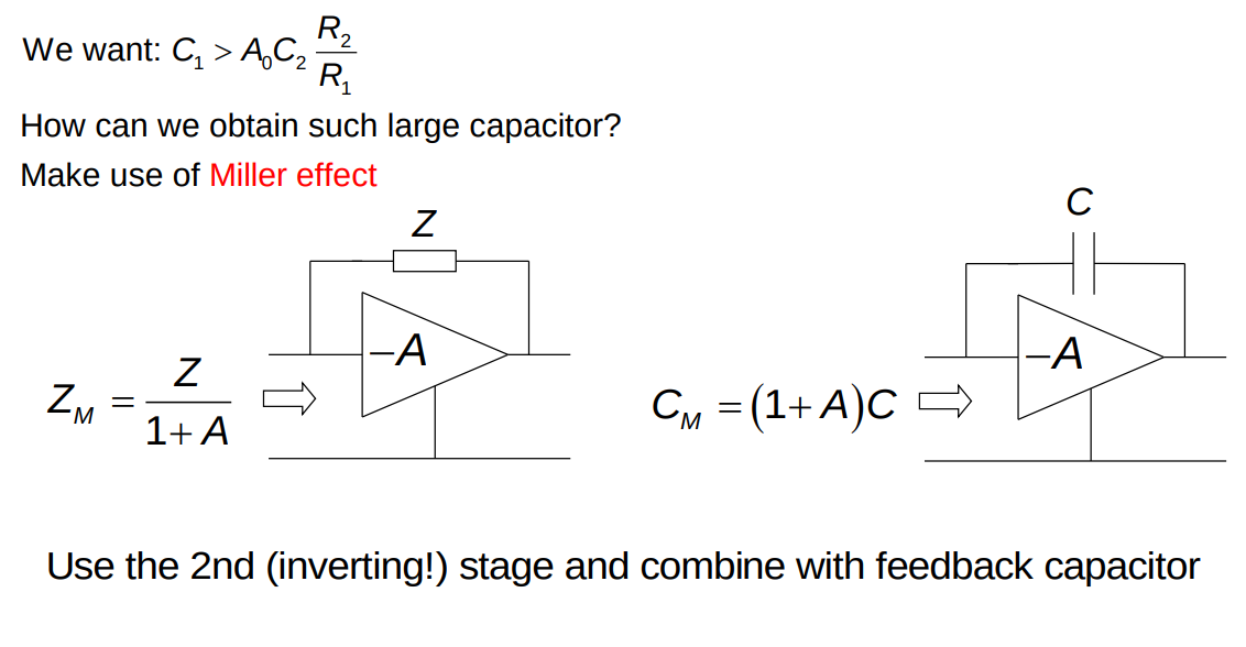
we want:
so we want
→
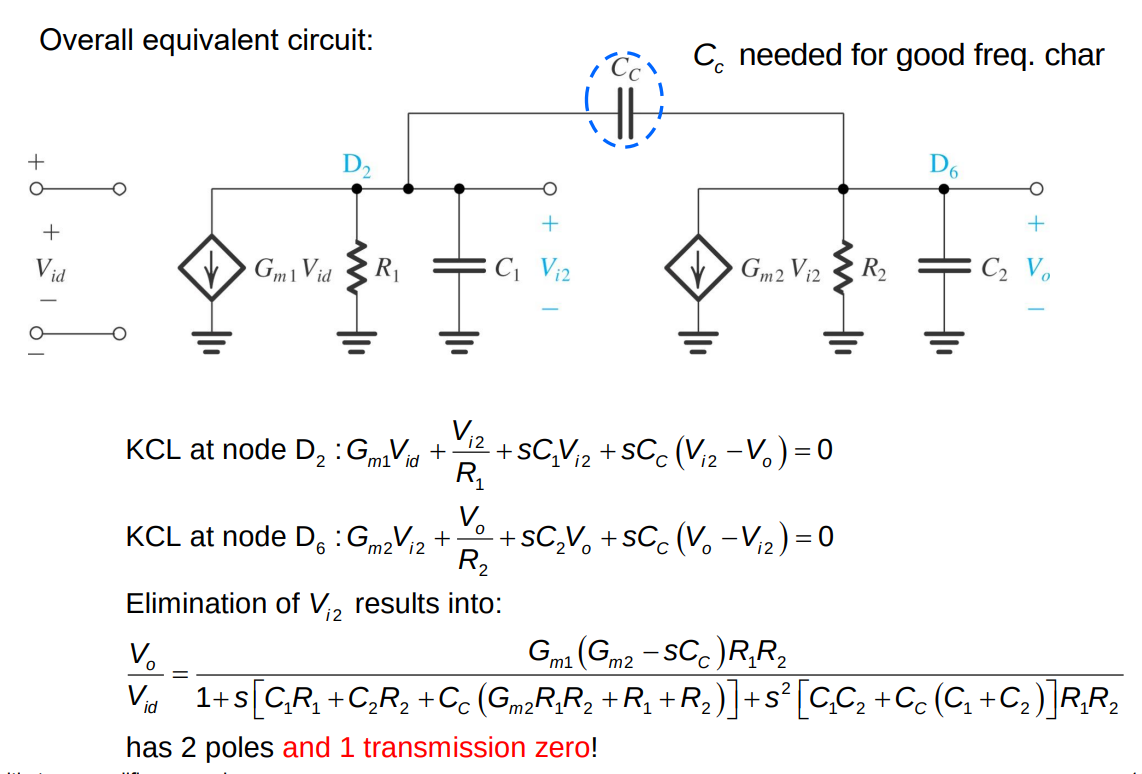
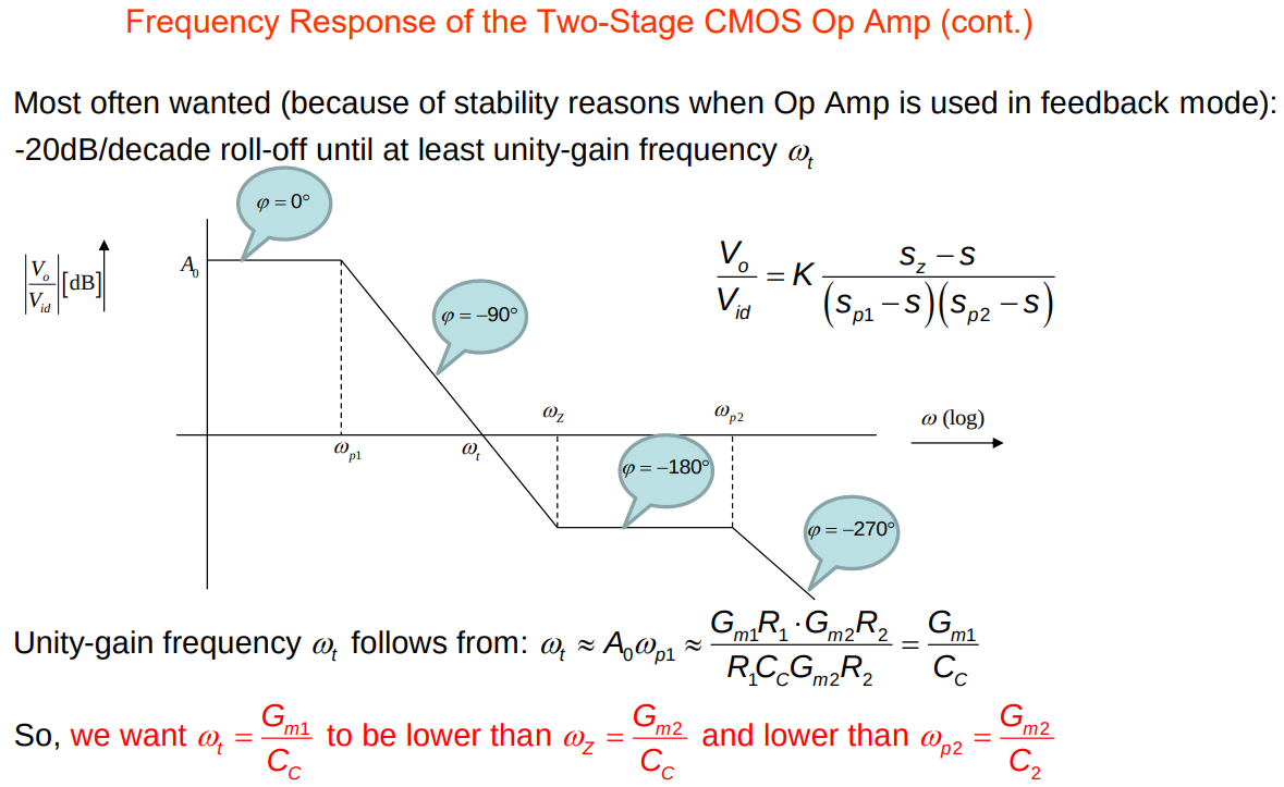
- pole splitting when they were close they were rotating phase
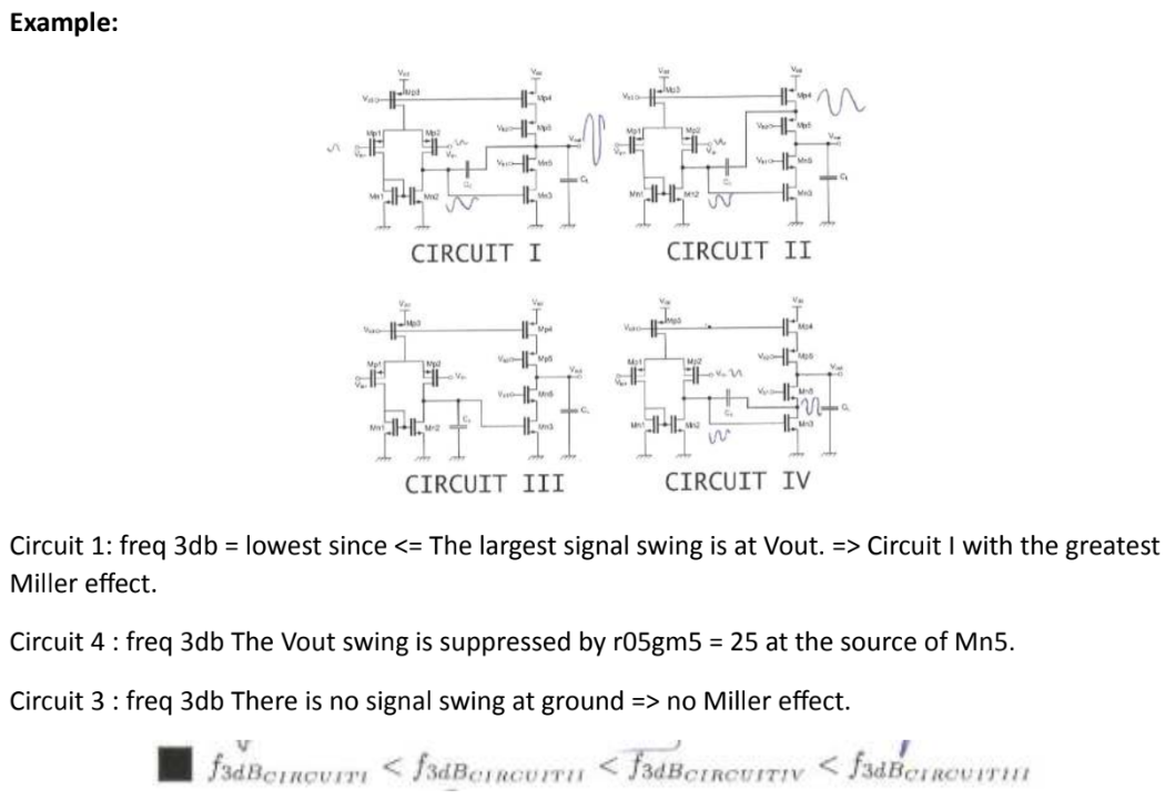
, now they are further apart as one becomes lower and higher frequencies. - transmission zero we have a zero when 2 parts arrive at certain point, these 2 parts have different transfers, there can be point in frequency where they cancel each other. since we add miller capacitance we give 2 ways for signal to reach output. We must control the zero, we can add a variable resistor after
. At high frequencies (1 stage amplifier, C low impedance path, MORE STABLE, diode connected transistor) we can assume that the path shorts the other, at low frequencies (C path is high impedance, gain of both stages, MORE GAIN) it takes the path where the signal has high gain.
miller effect:
→
since we have a diode connected transistor to
→
- (note:
as includes load capacitance) - transmission zero
has two negative real poles:
- In total the negative phase shift can become large→dangerous for stability!
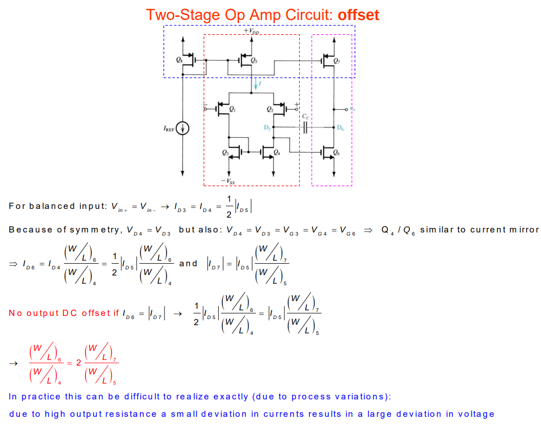
no output DC offset:
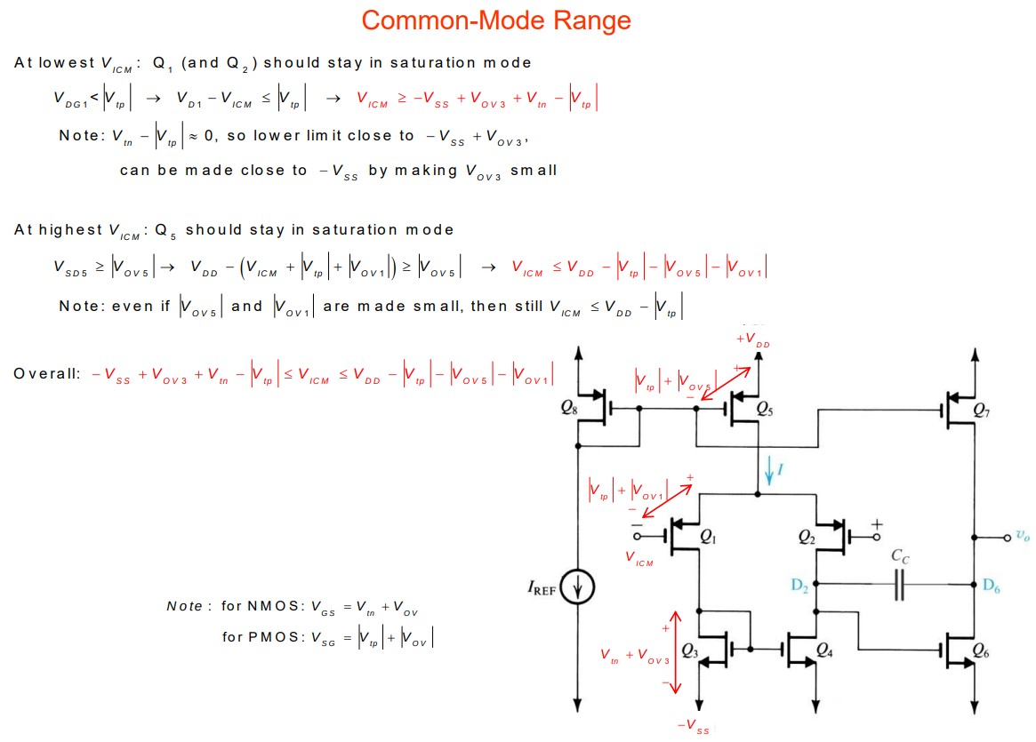
Common mode range
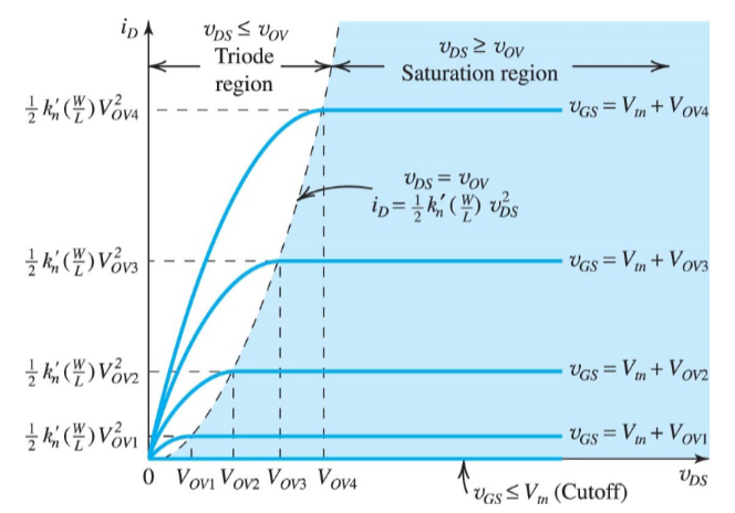
saturation mode: NMOS:
,
Small signal voltage gain
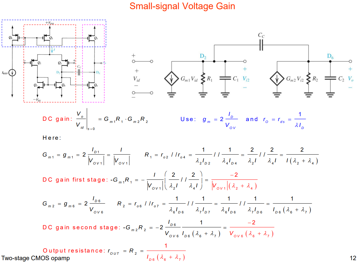
DC gain first stage:
DC gain second stage:
Common mode rejection ration
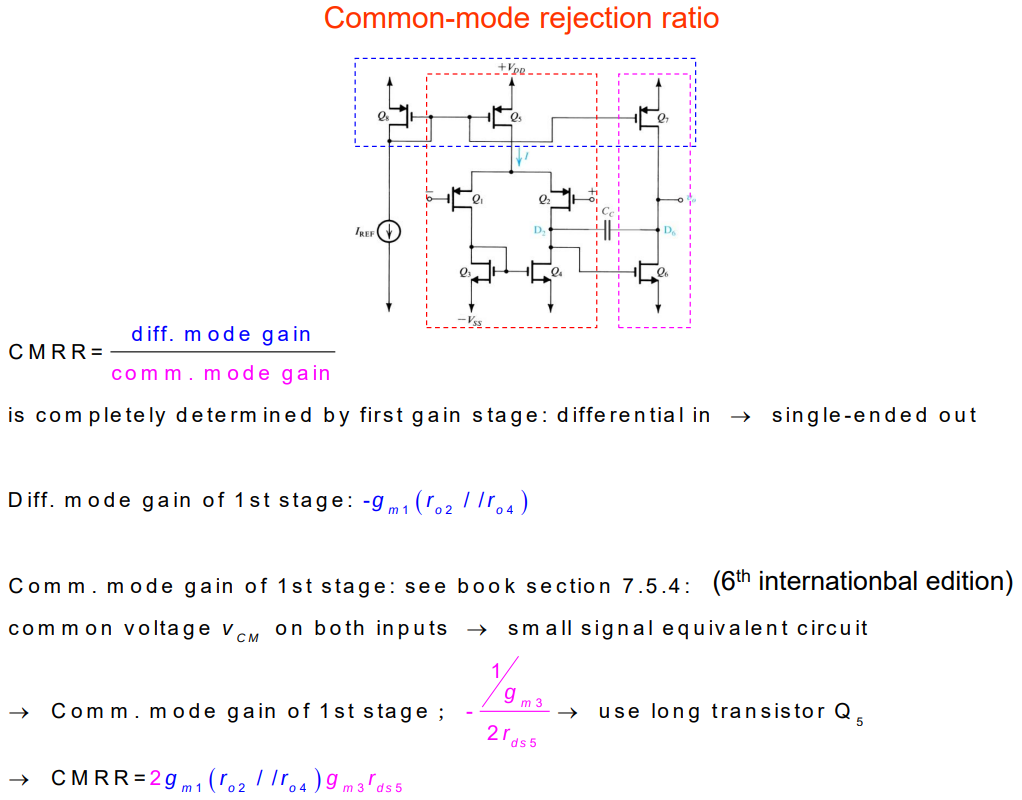
diff mode of 1st stage:
comm mode of 1st stage:
If Q1 and Q2 change than Q5 modulates in common mode, which modulates the current, due to channel length modulation. This makes the drain current of Q1 and Q2 modulate, Q3 copied to Q6 with an error, because of finite gm of Q3 transistor.
The error at D6 is the error different between current of Q2 and Q4, at D6 its translated to voltage through resistance level at this node. → common mode gain.
Frequency response
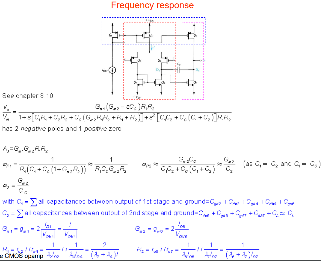
Phase margin
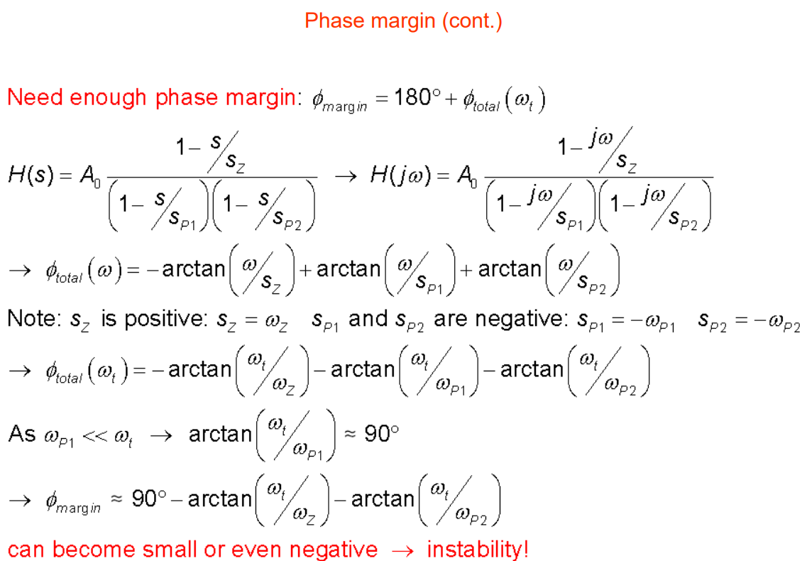
poles and zeros manipulation allows for designing the circuit to achieve specific frequencies.
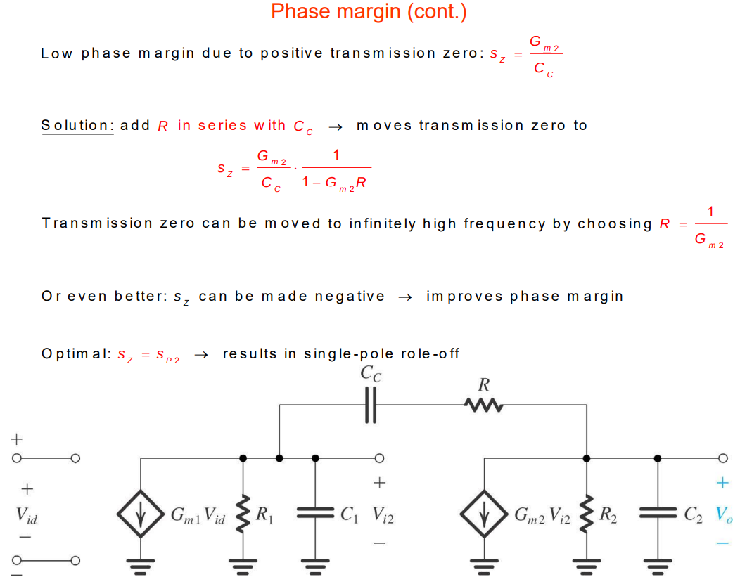
adding R →
Slew rate
maximum range at which the output voltage changes

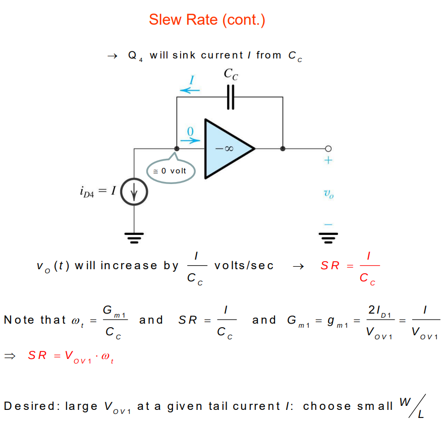
Power supply rejection ratio
reject disturbances from power supply to the voltage
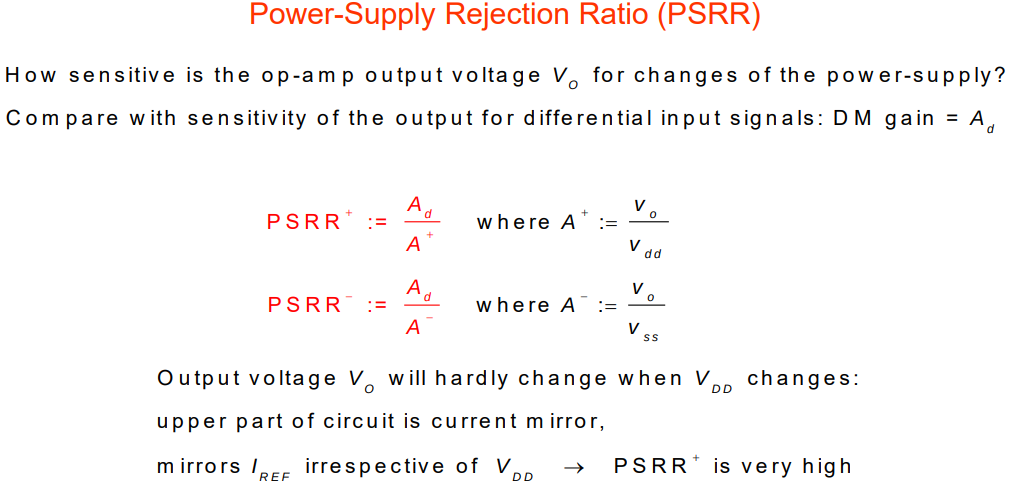
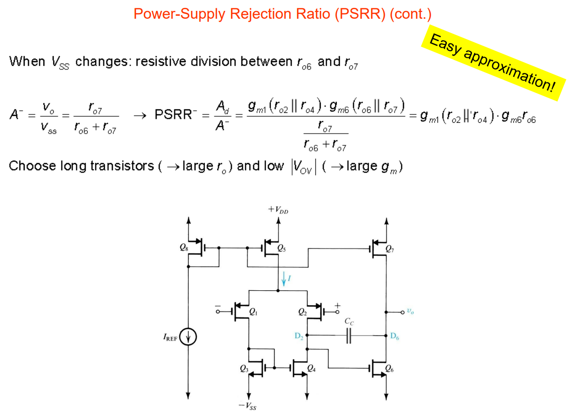
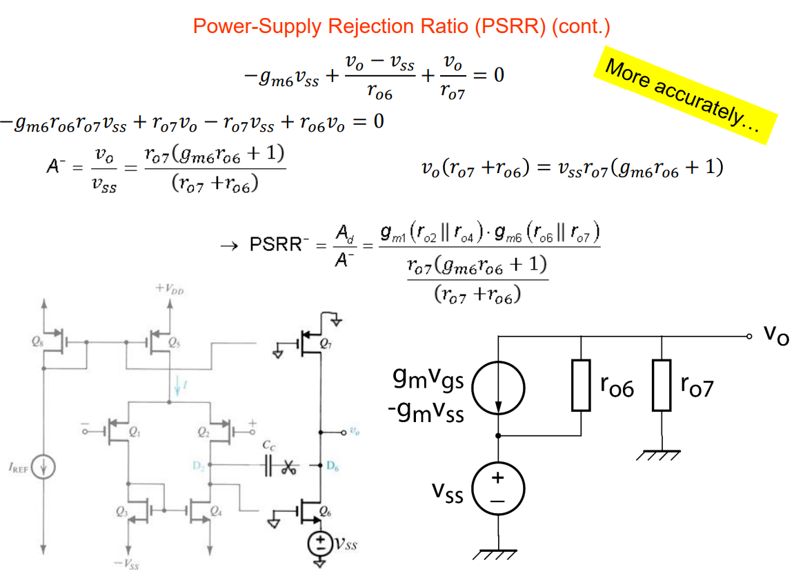
first psrr calc:
CMOS Class AB output stages
- ideal current source:
while ideal voltage source - output stages should have:
- large output voltage swing
- large output current range
- low output impedance
- little distortion
- good power efficiency
- switch and linear mode, class D switch mode: transistors used as switches if ideal switches they are efficient.
- How to distinguish between classes of linear-mode output stages? Observe drain (or collector) currents of output stage for sine wave input.
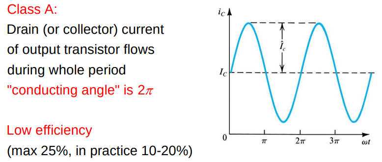
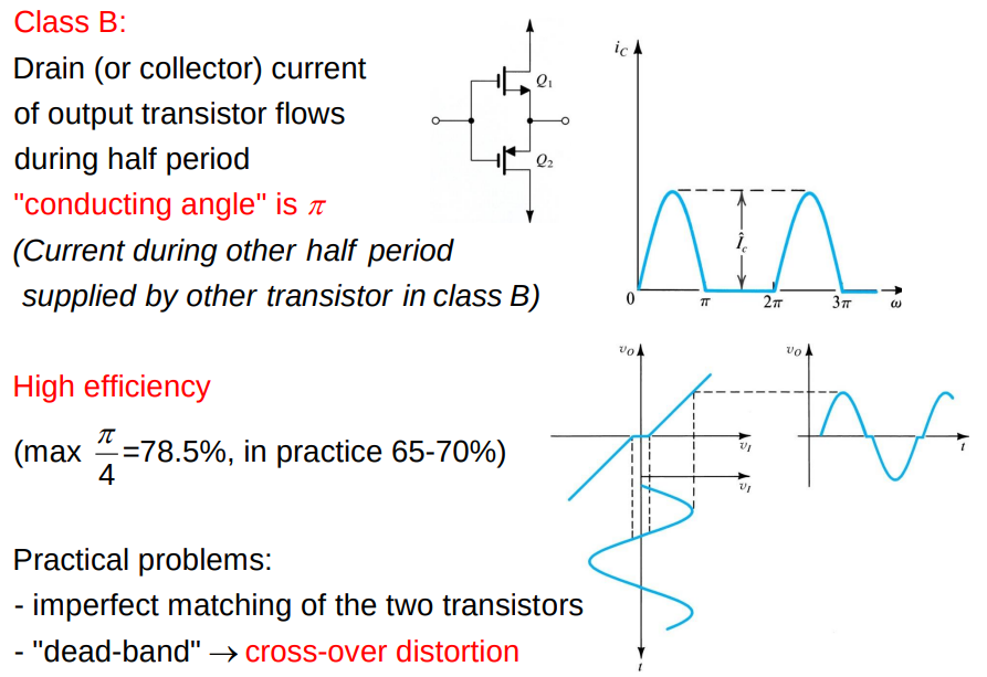
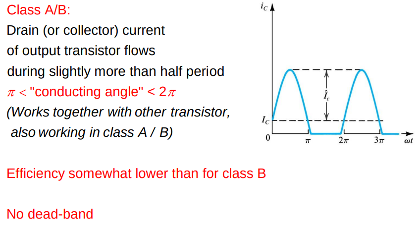
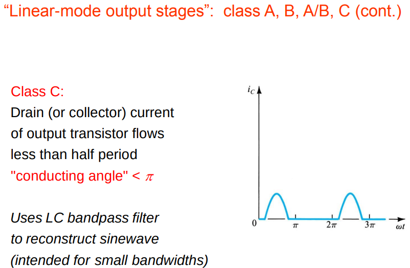
To avoid deadband in classical AB connection we have:
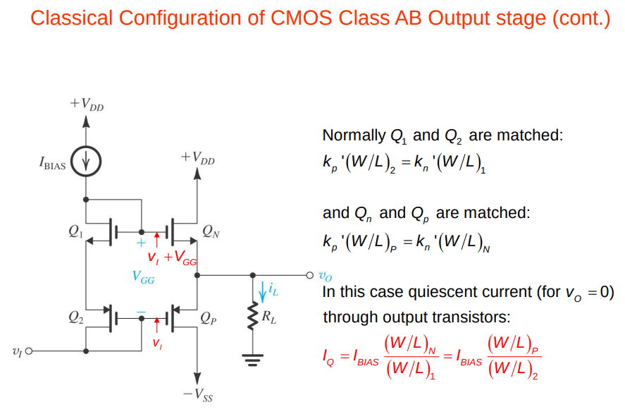
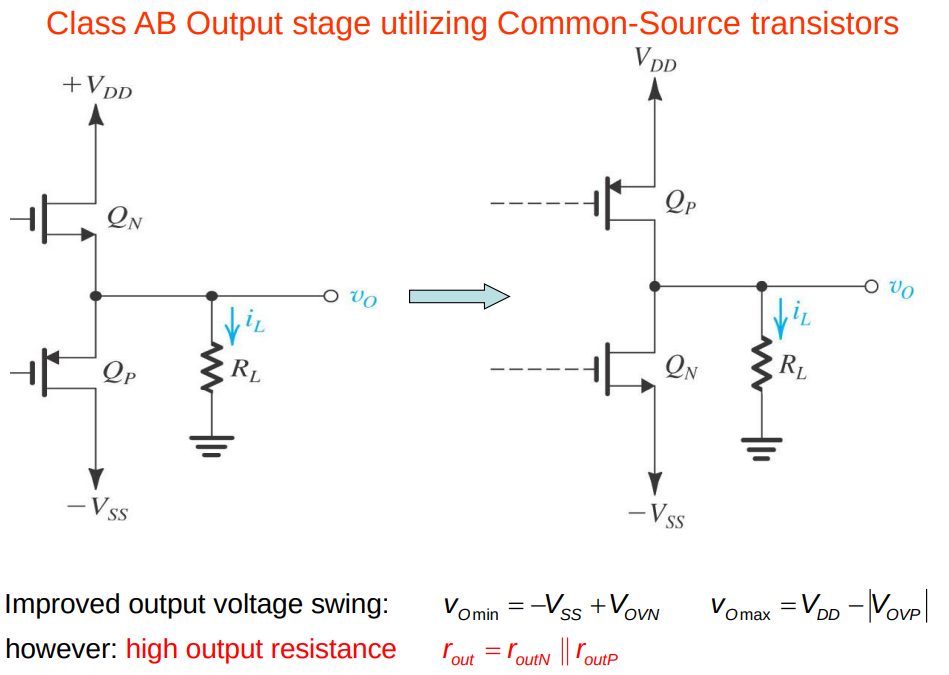
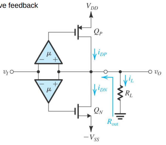
output impedance can be decreased by negative feedback:
similarly for
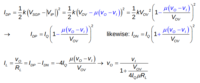
gain error:
so:
when matches transistors we have the same current so
Data Converters
Topic: Data Converters
Data representation
adc, dac: https://www.youtube.com/watch?v=HicZcgdGxZY
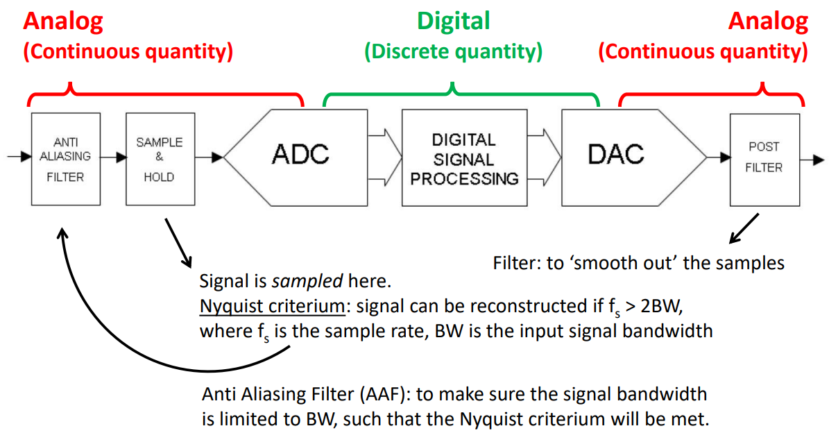
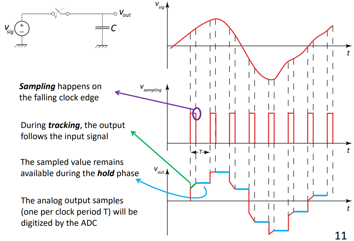
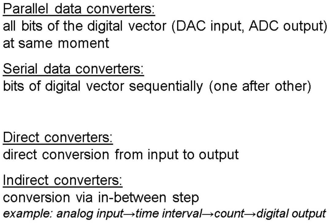
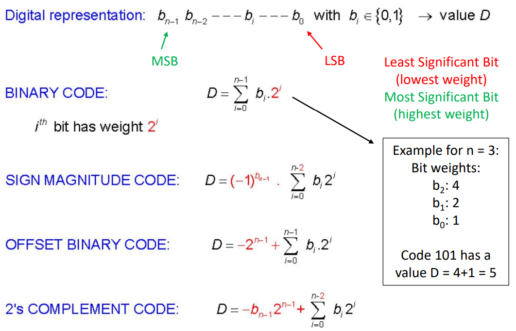
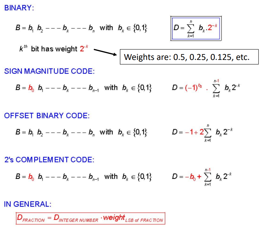
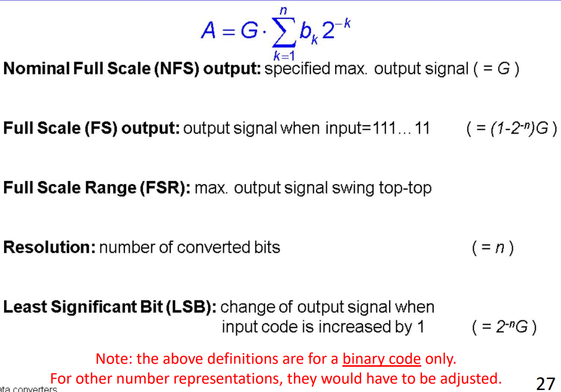
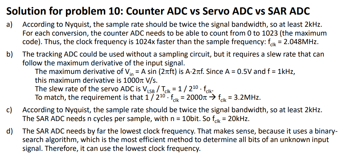
- Nyquist: sampling frequency must be at least double. anti aliasing filter used to make sure.
- clock period:
- binary doesn’t have negative, sign magnitude LMB 1→-, 0→+, offset additional offset , 2s compliment invert binary string and then +1 and then result is same as sign magnitude.
similar to above for integers but for instance 001 → example: → A is analog output 
- offset if 011001: 16+8+1-32=-7
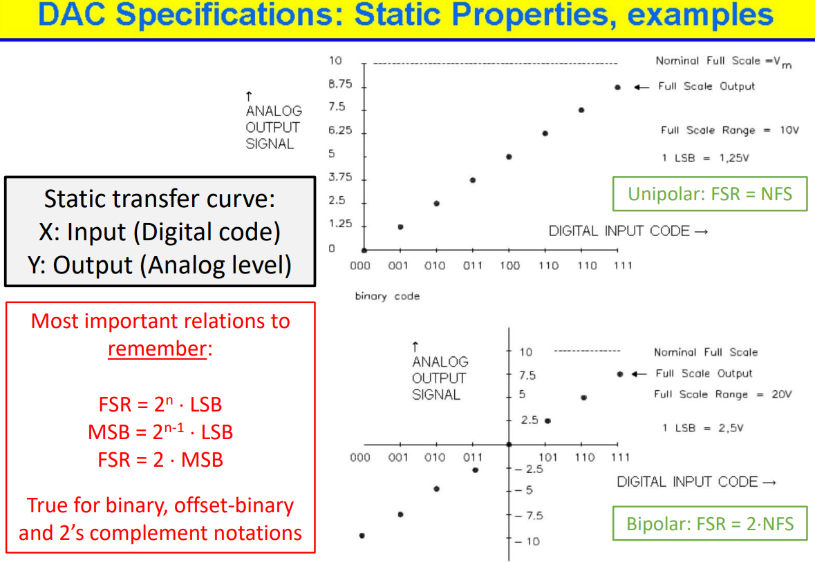
FULL SCALE RANGE
→NOMINAL FULL SCALE range which is half of
STATIC ERRORS:
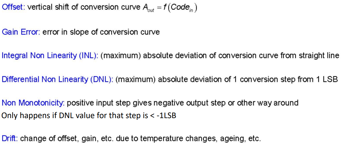
- INL you can make a curve graph showing the absolute deviation which plots the distortion curve. From curve you can take absolute min max val to find INL. Causes non-linearity.
- INL is integral of DNL
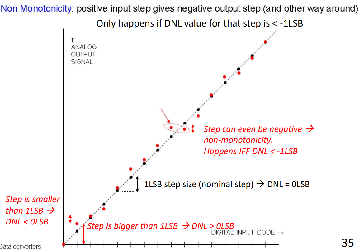
- ideal steo should be 1 DNL but if the actual isn’t and is smaller than -1LSB since the step moves down…:
DYNAMIC ERRORS:
Settling time: time it takes between:
- input changing from 000..00 to 111..11
- output signal stabilizing within 0.5LSB from final value
Slew Rate: maximum speed with which output signal can change
SFDR-(spurious free dynamic range): difference in height between:- wanted spectral peak (due to sine wave at input)
- highest unwanted peak (= spurious tone)
DAC
Weighted resistances Network
summery: https://www.youtube.com/watch?v=PoOm_G4s1dE
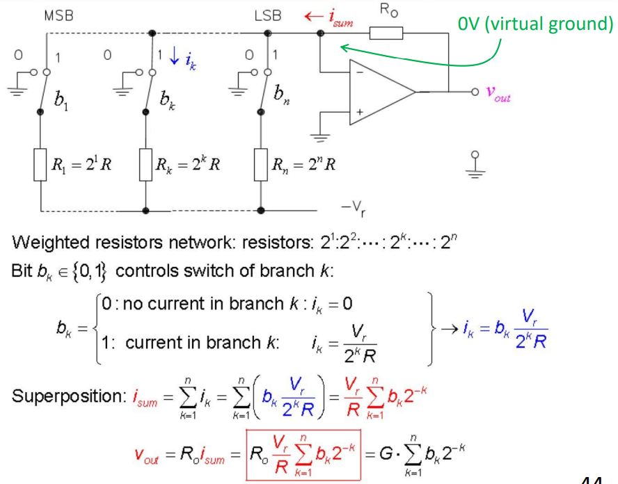
if switch ON or OFF the voltage at that node is always zero, since inverting amplifier always equates to virtual zero at the two branches so we have
when:
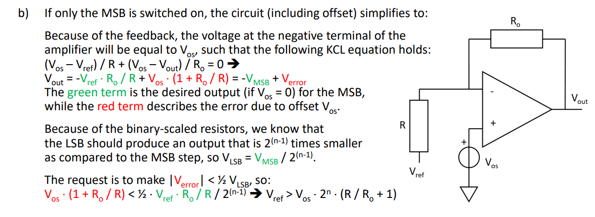
MSB: smallest resistor, largest current (left side)
LSB: largest resistor, smallest current (right side)
binary weighted resistors→binary weighted currents
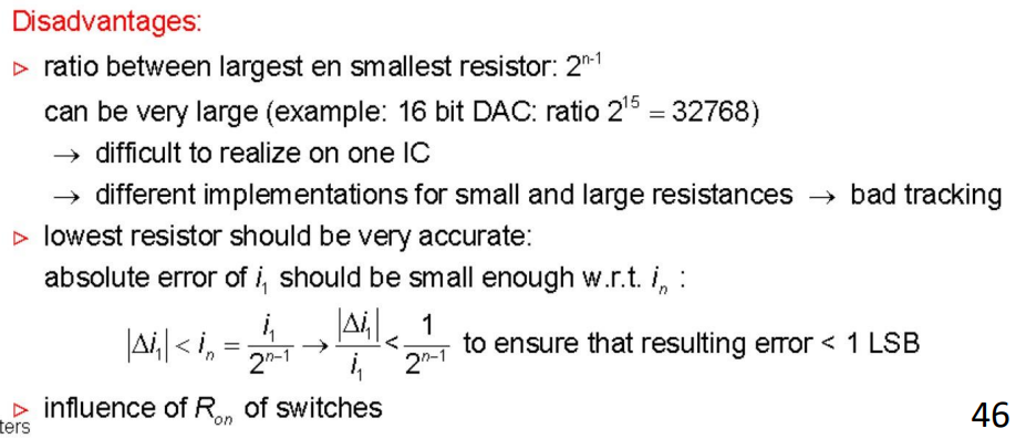
- as NUM of bits increases NUM of resistors increases, and if they are not accurate can cause error in output…
example:error must be less than that percentage for 10 bit converter. so we have to increase the amount of resistors in the circuit which is hard to achieve that’s why we have, for high accuracy high resolution:
R2R ladder
summery: https://www.youtube.com/watch?v=Pc1aFloxSMw
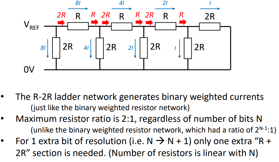
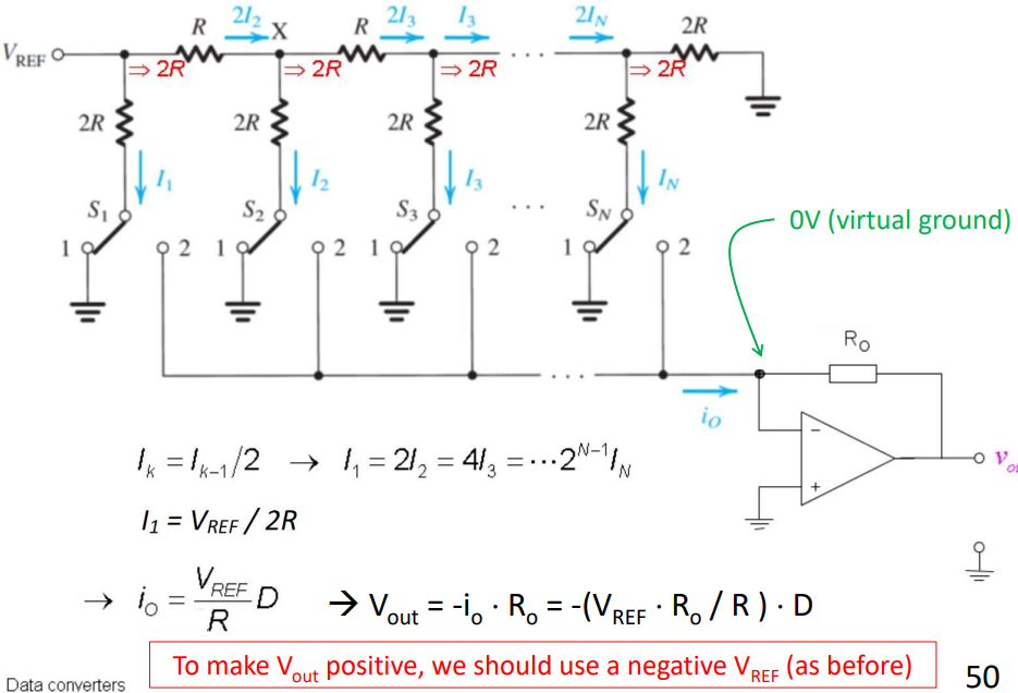
we calculate the first block:
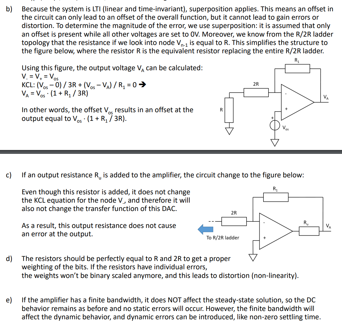
if deviation:
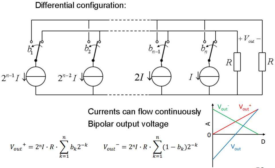
summation can also be done with KCL using current sources:
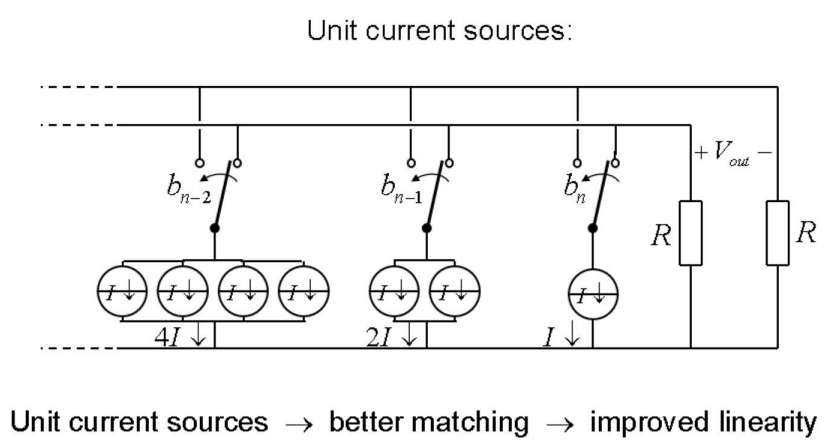
we can also use triode transistors where the source is
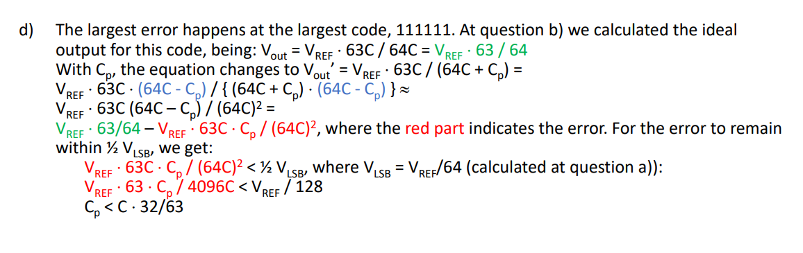
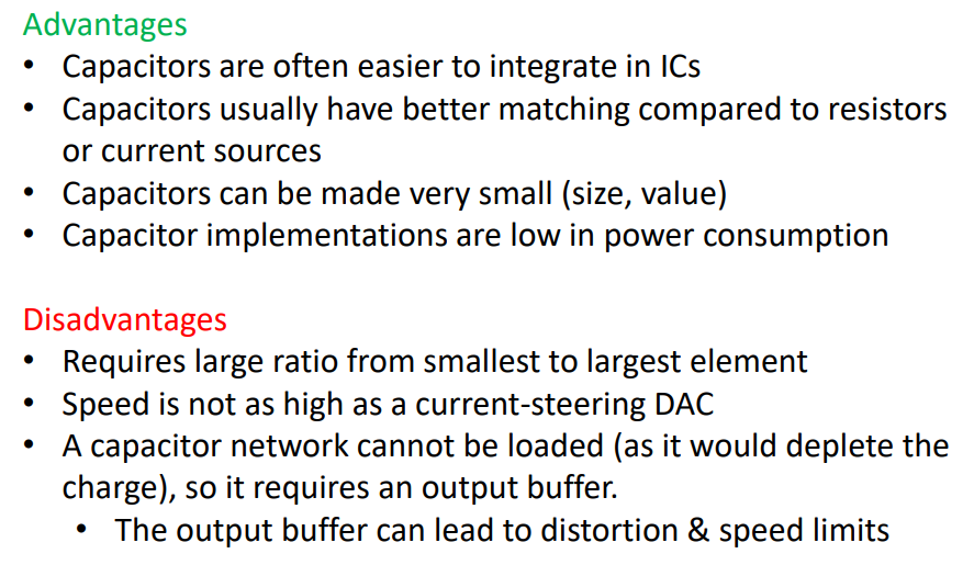
Charge – redistribution DAC
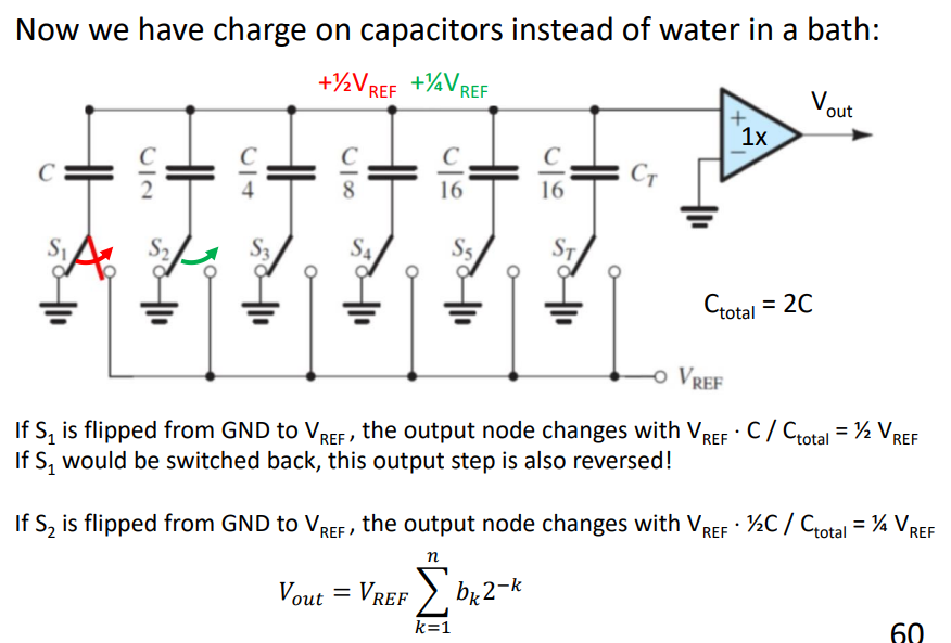
if all off and then we turn on lets say S4:

ADC
Specifications
non-linearity: https://www.youtube.com/watch?v=TTO35V3XgiU
It will face the same non-infidelities as DAC +:
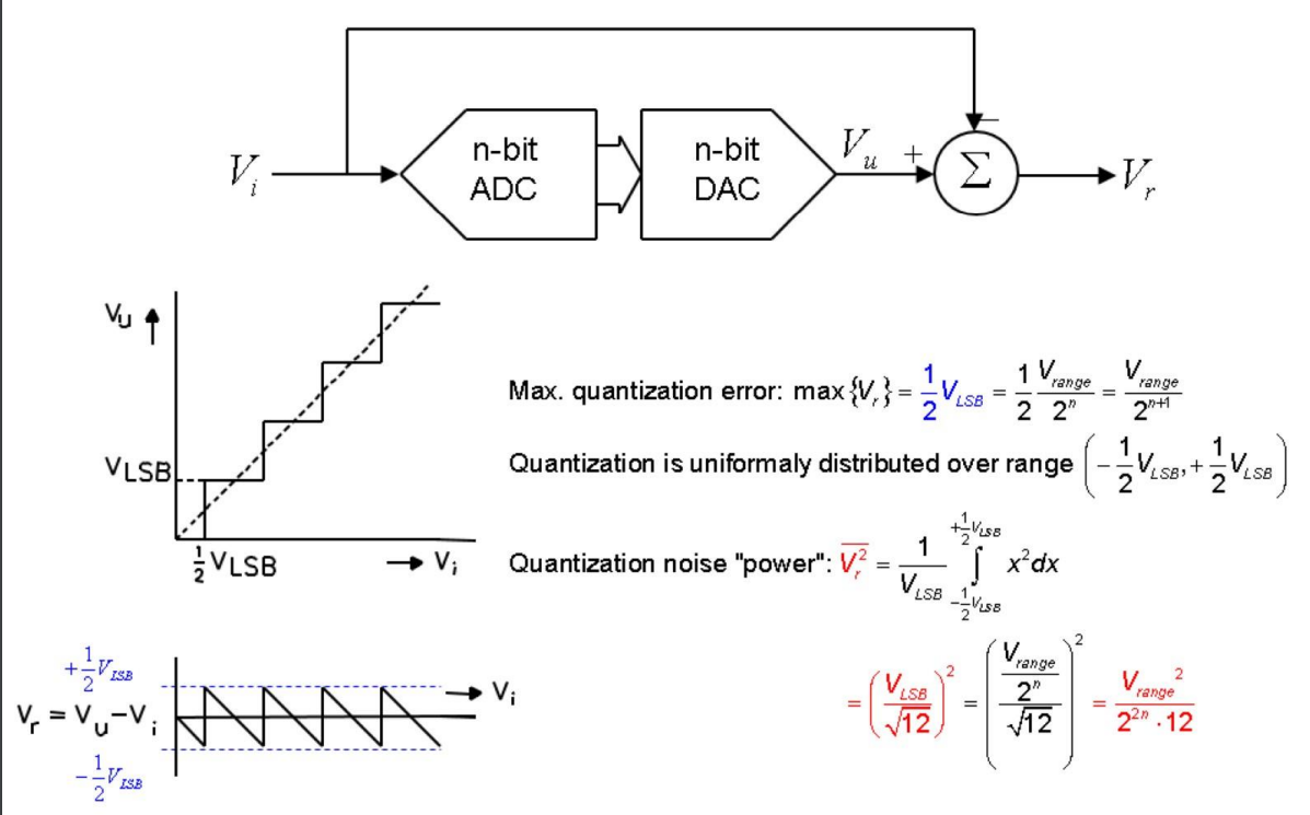
Quantization Noise (power):
max amplitude:
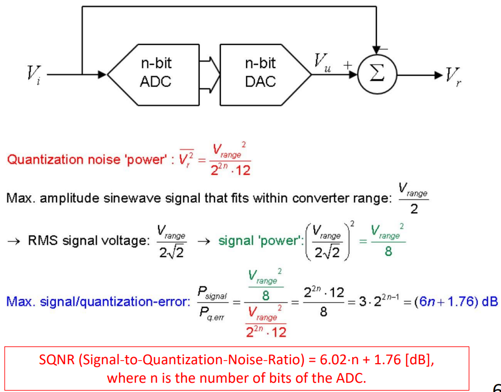
MAX signal quantization error:
SQNR (signal to quantization noise ratio)→where n is number of bits in ADC
there is also a non-linearity when quantization is larger than the
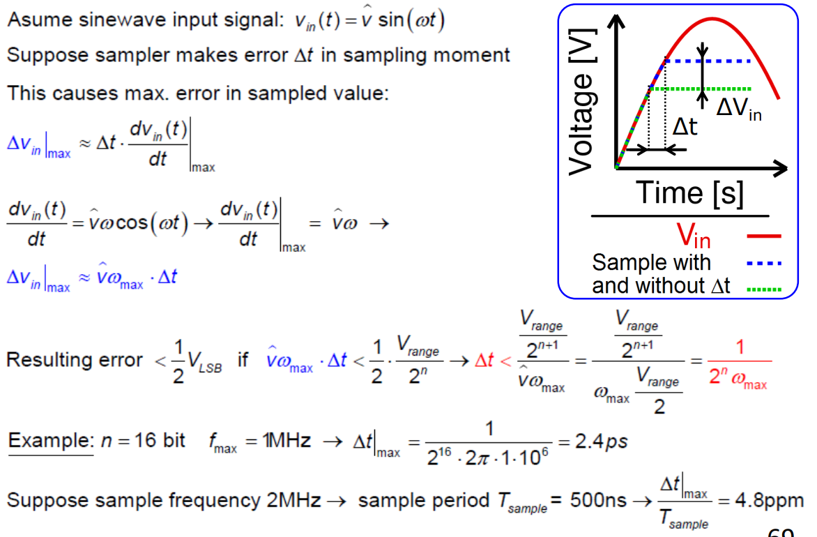
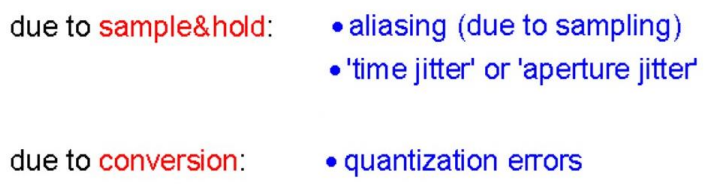
max error in sampling:
we must keep it
to have no aperture jitter:
Flash ADC
https://www.youtube.com/watch?v=NASkjo7s8f4&t=1s
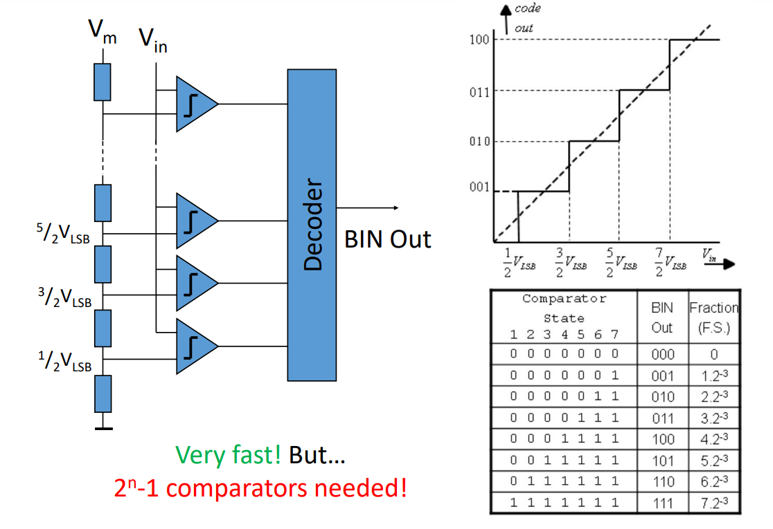
- very fast
comparators needed as you increase bits
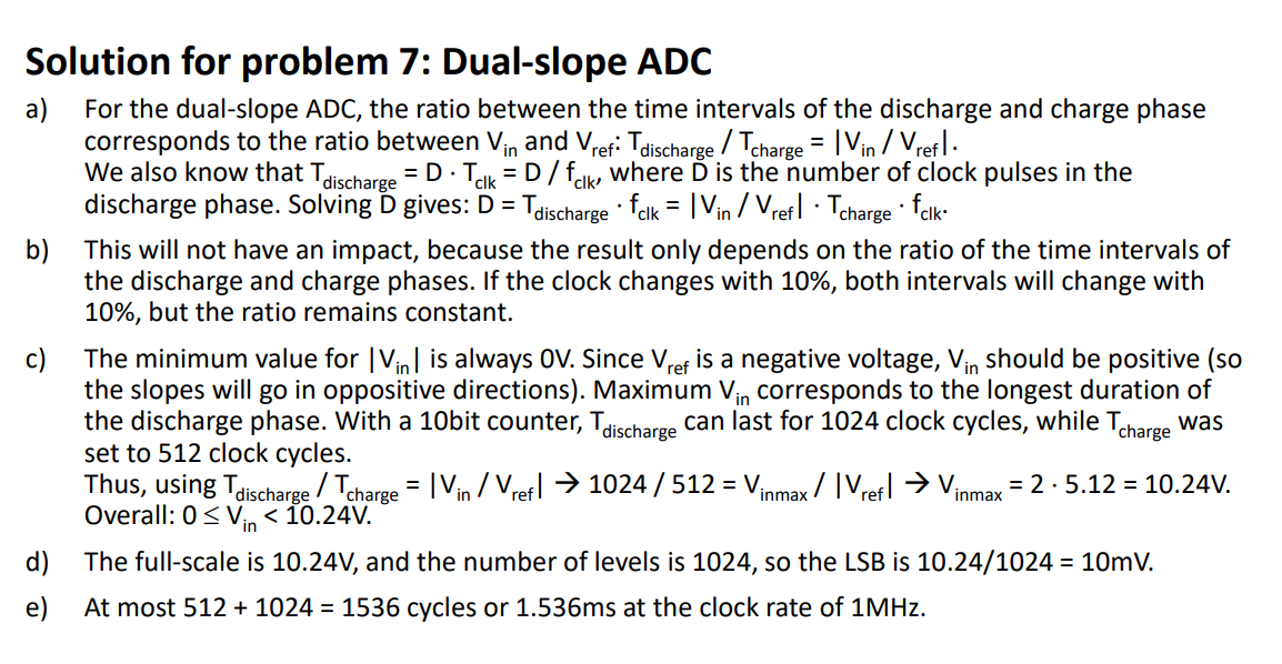
Slope ADC
https://www.youtube.com/watch?v=2gF_nfaBV_0
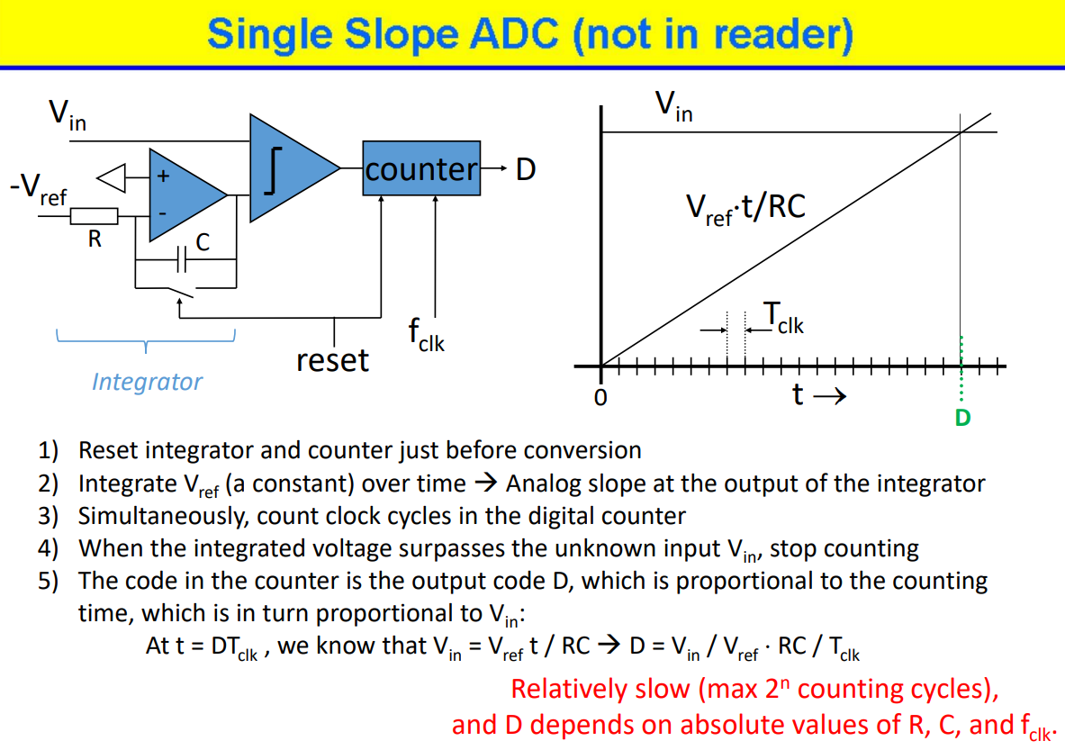
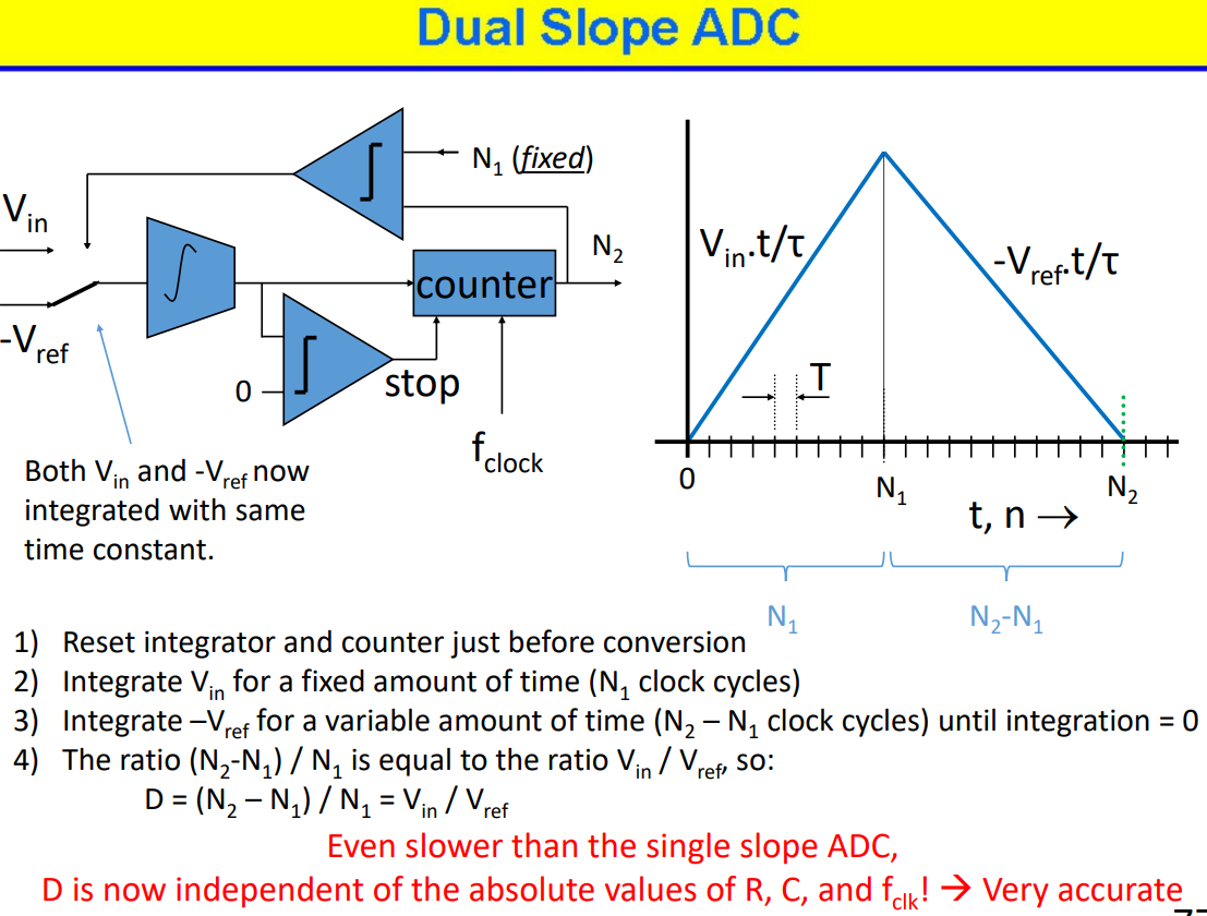
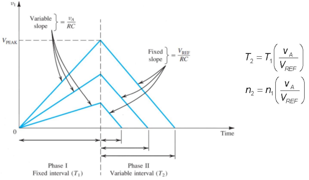
- slower than single slope
- very accurate
- error in capacitance or clock freq does not result in an error in the conversion of the D
conversion time:
integrator voltage:
Counter & Tracking ADC
counter: https://www.youtube.com/watch?v=4zwtA2pG6Vc
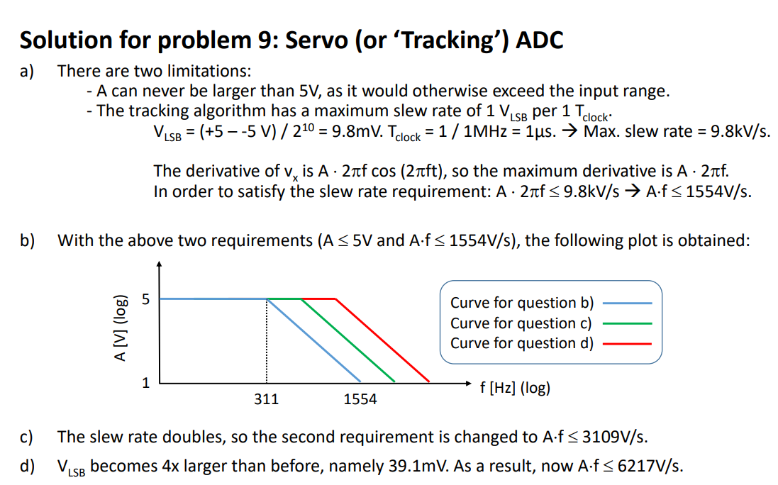
tracking: https://www.youtube.com/watch?v=MMQwa416Cmo
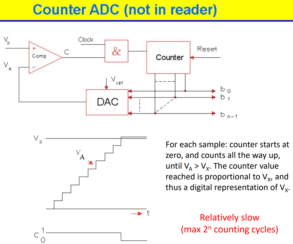
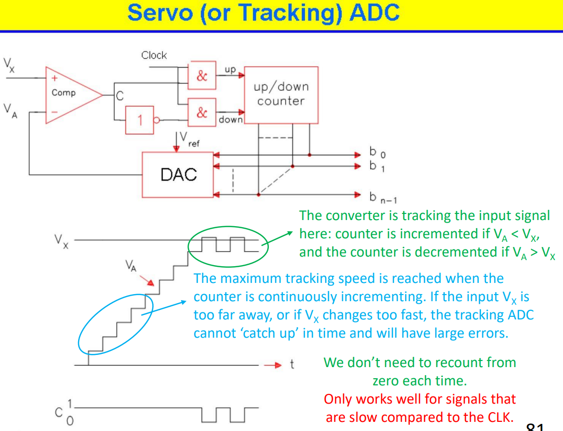
tracking: Looks similar to counter ADC, but instead of resetting the counter to zero at the start of each conversion, the counter value is maintained, and simply incremented or decremented at each clock cycle to follow (track) the input signal.
Successive Approximation ADC
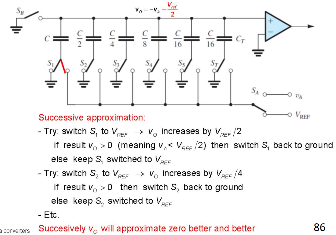
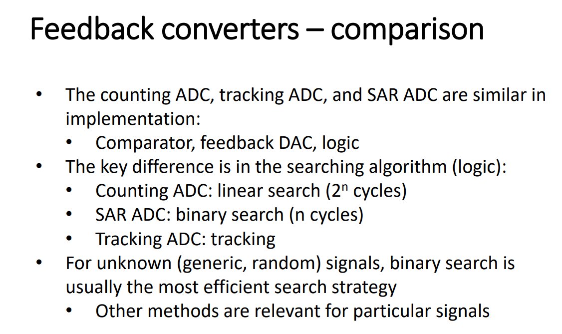
- For an n-bit ADC, n cycles are sufficient (as compared to
cycles for the slope and counting ADC). is applied to all capacitors. - Requires only as many search cycles as we have bits: an n-bit SAR ADC needs n search steps.
 CMOS digital logic circuits
Topic: Digital Logic
CMOS logic Circuits Dynamic Operation of the CMOS Inverter
Basics
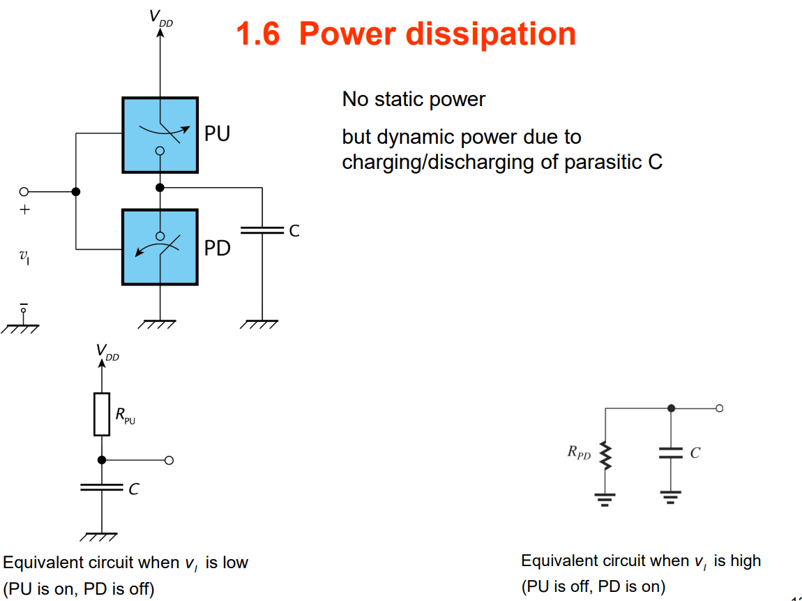
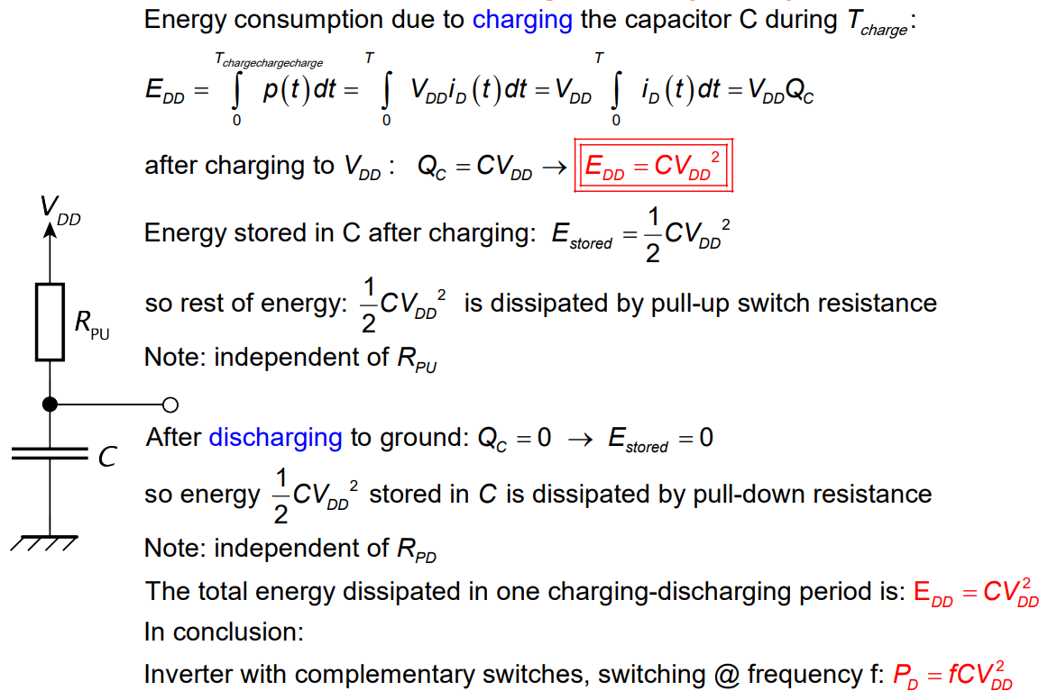
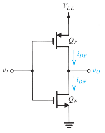
Energy dissipated in one charging-discharging period:
Inverter with complementary switches, switching @ frequency f:
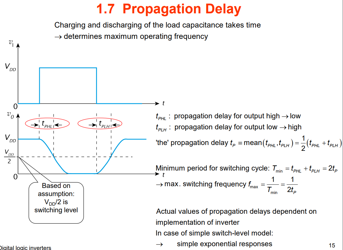
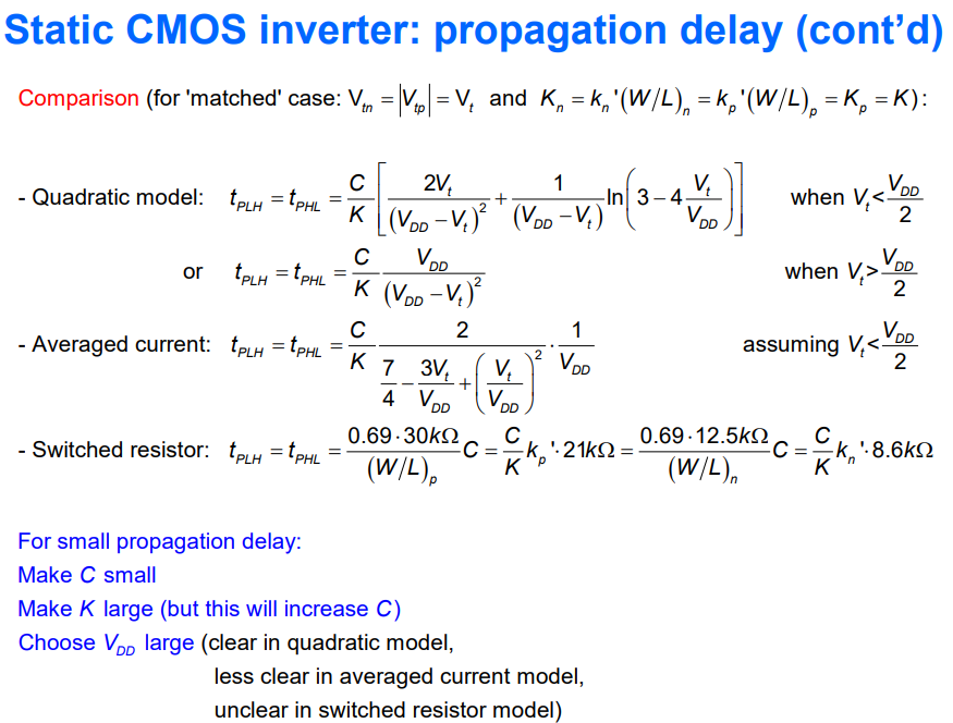
Propagation Delay
Power-Delay Product ( PDP):
Inverter with complementary switches:
worst case PDP when f is max
PDP doesnt reflect propagtion delay
Better FoM: Energy-Delay Product ( EDP):
1st order circuits step response:
⇒
same…
it could also be that one opens and the other closes which means:
can also calculate the propagation delay graphically:
example:
⇒
CMOS Inverter
Basics
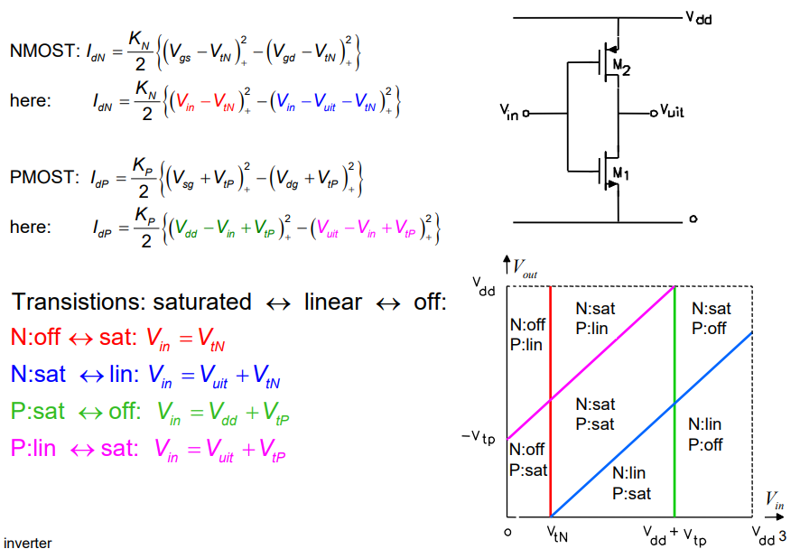
you can draw the line through this matrix as derived in week 7 slides conclusion:S
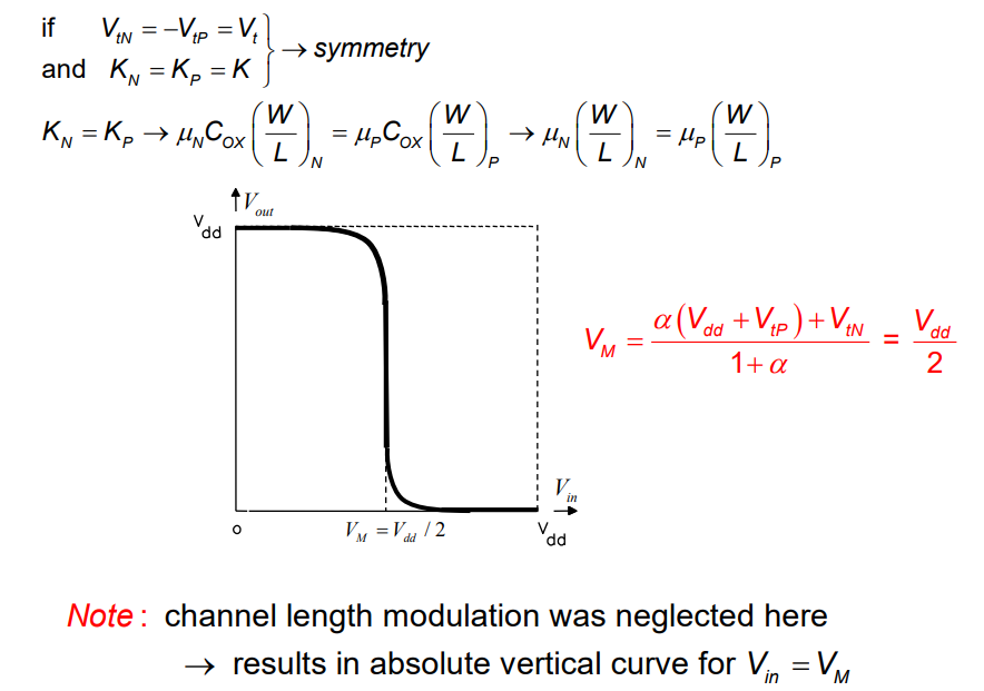
trip voltage
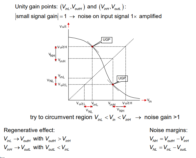
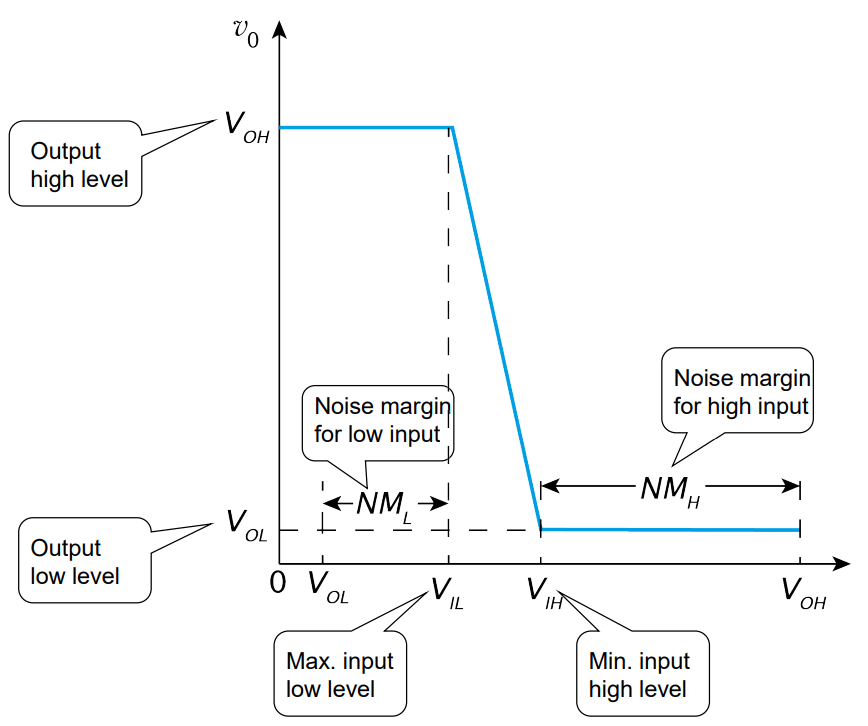
Noise margin=
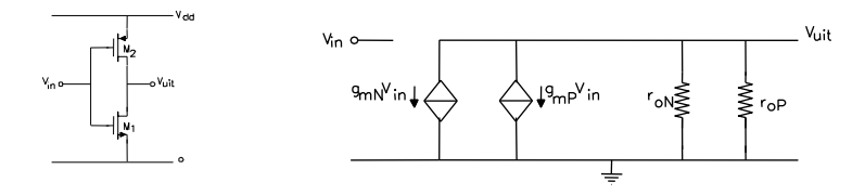
for symmetric configurations:

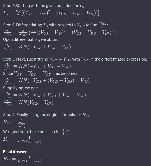
Pull down resistance(at NMOS):
where:
so then:
SUMMARY
and
and
and
static power max: 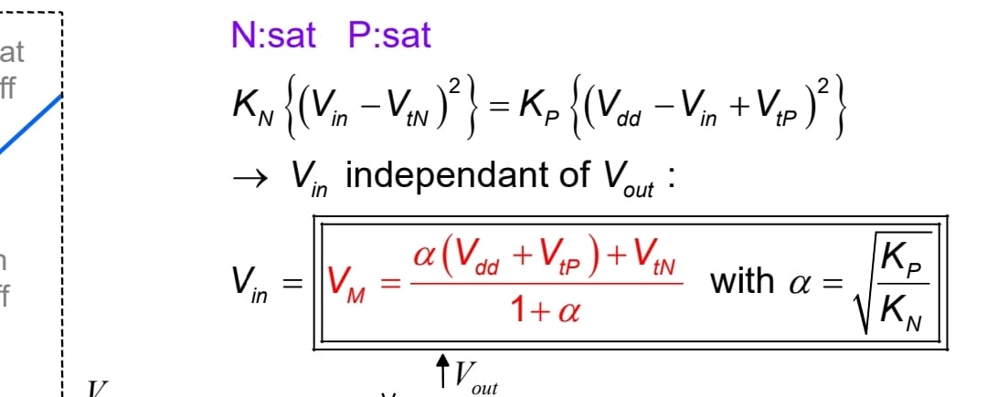
frequency of ring oscillator:
equivelant load capacitance:
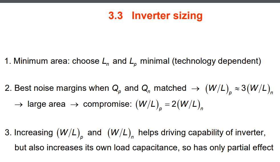
Static CMOS Inverter

take into account
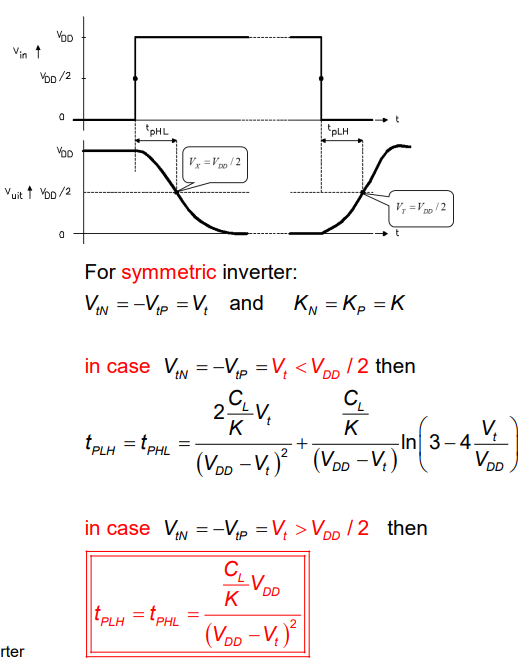
there is 2 other methods you can find in formula sheet…
CMOS Digital Logic Circuits
Basics
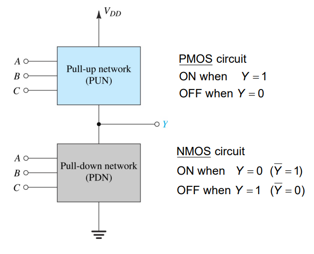
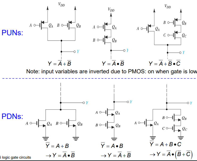
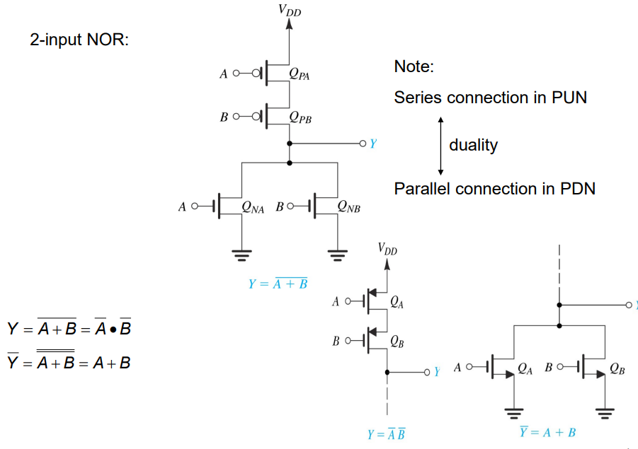
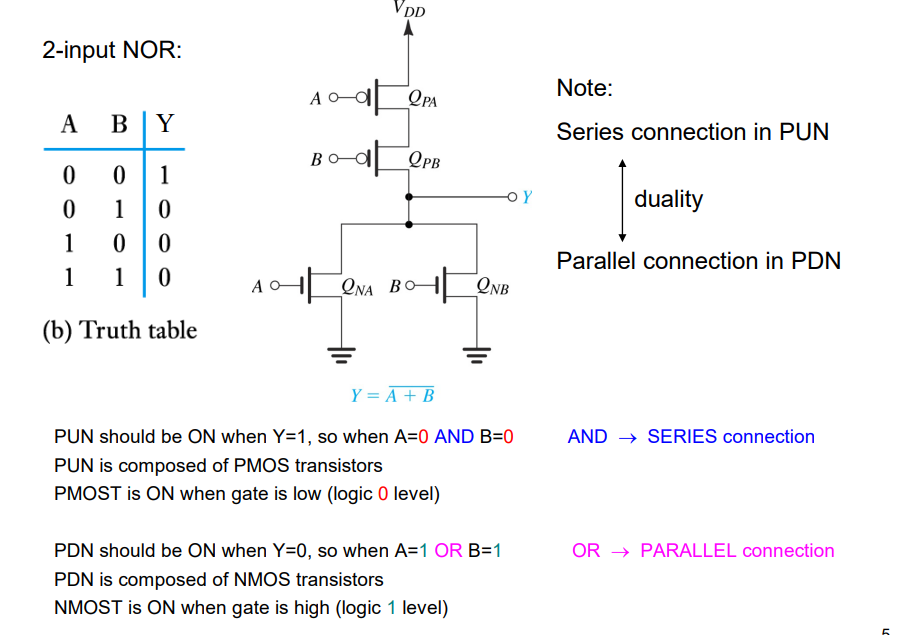
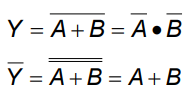
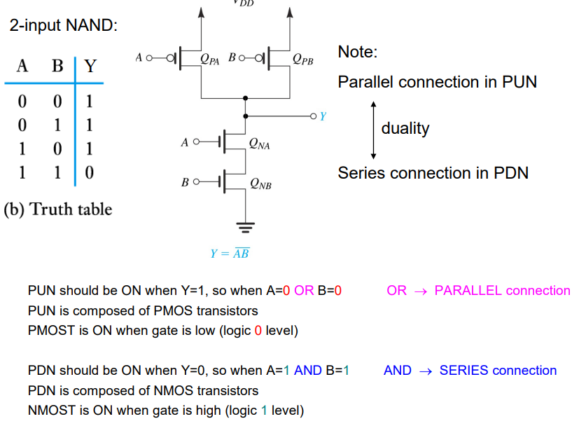
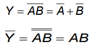
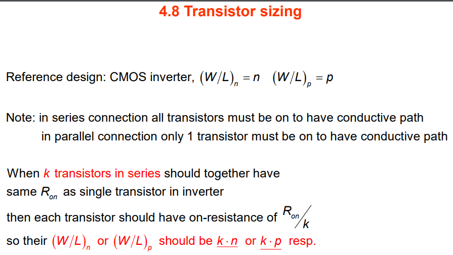
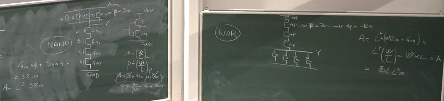
NOR || NAND
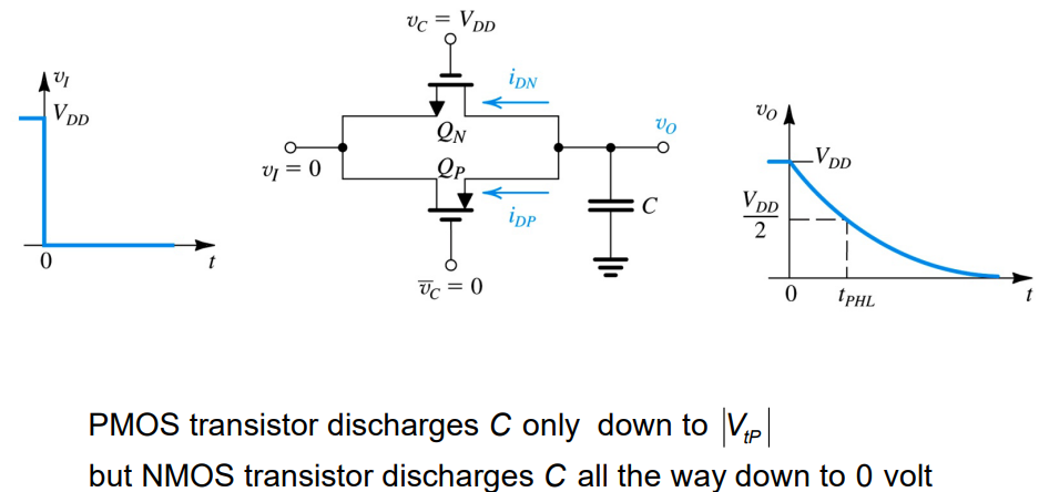
CMOS Transmission Gates as Switches
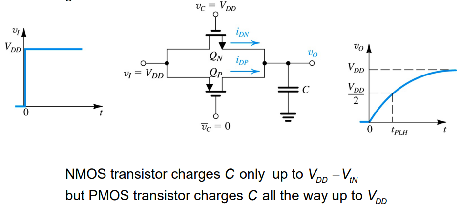
- Transmission gate can be used as a (floating) switch, of which the state (on or off) can be controlled by a voltage
- NMOS transistor charges
only up to - PMOS transistor charges C all the way up to
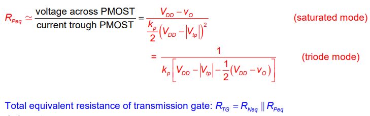 empirical approximation:
as is quite constant over
Memory Circuits
Topic: Digital Logic
Static memories
it remembers its input, and therefor to reset it you would have to reconnect power.
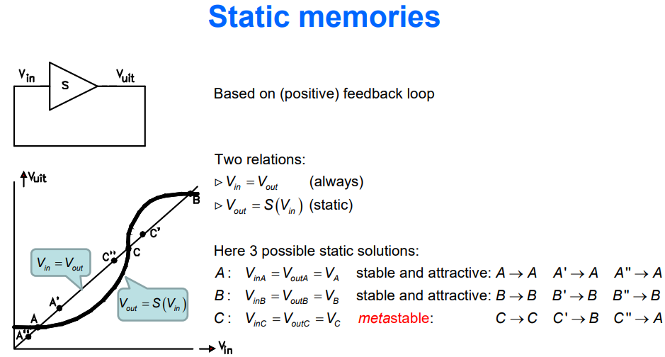
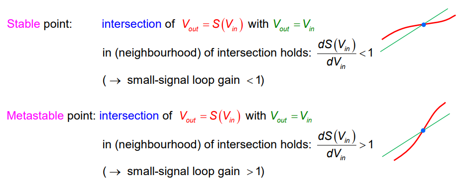
The Latch
dynamic memory
latch: https://www.youtube.com/watch?v=KM0DdEaY5sY
flip flop: https://www.youtube.com/watch?v=F1OC5e7Tn_o
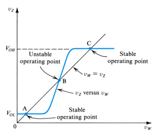
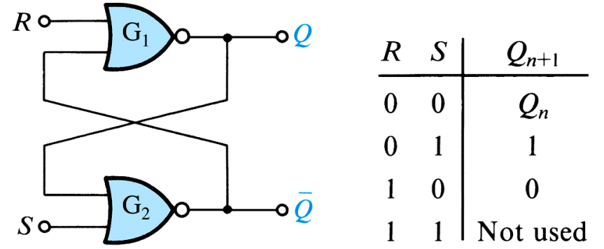
R: reset, S: Set
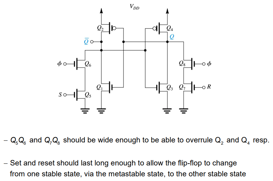
With the SR flip flop we are able to have more control and remove the 1 1 error, by having a clock speed to trigger the changes same as the latch. Due to a capacitor there is only at trigger when there is that quick discharge moment from the signal at the start, check video. There different flips flops check slides for further info.
Static Memory SRAM Cell
SRAM: https://www.youtube.com/watch?v=veJs793zvz4&t=49s
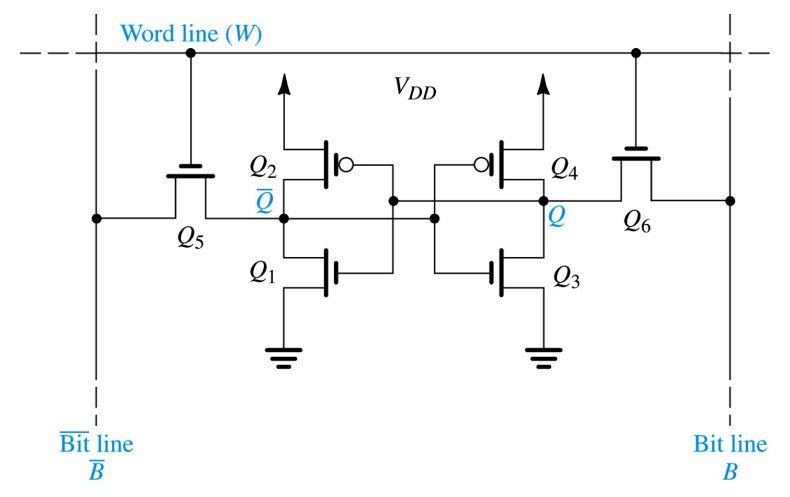
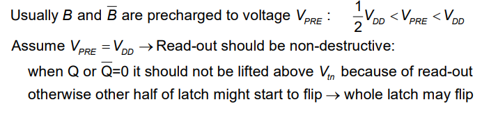
READ OPERATION:
WRITE OPERATION:
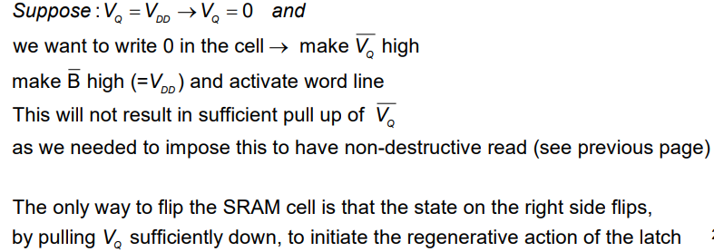
The only way to flip the SRAM cell is that the state on the right side flips, by pulling
Dynamic memory cell
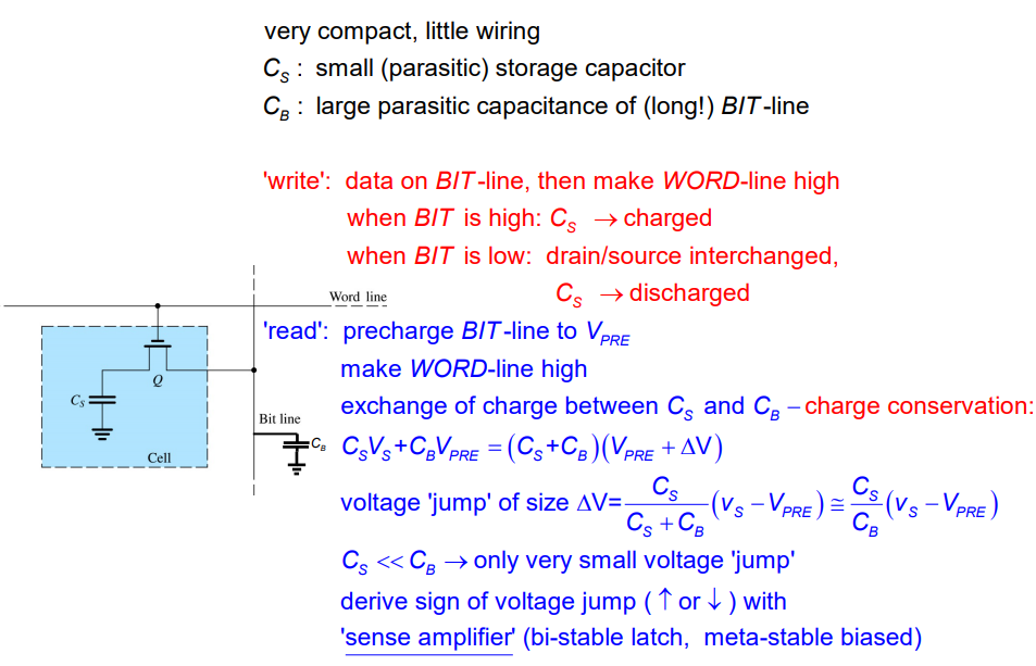
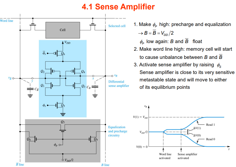
ROMs are floating gate transistors, see slides it stores permanently above the channel.