5ECB0 Electronics I
- Area: Electronics
- Topics: Semiconductors and PN Junctions · MOSFET · Transistor Amplifiers · Current Mirrors · Differential Amplifiers · Operational Amplifiers · Oscillators and Waveform Generators
- Related courses: Electronics II - 5ECC0 · Biopotential and Neural Interface Circuits - 5XCC0 · Photonics - 5XTB0
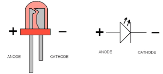
Carriers
Topic: Semiconductors and PN Junctions
- Intrinsic: electron-hole pair generated from thermal energy
- Doped: n-type (donor, n) and p-type (acceptor, p)
fixed (local) charge, globally neutral
and
and
Current
- Drift current: directional, ~E
- Diffusion current: ~concentration difference
P-N junction
Topic: Semiconductors and PN Junctions
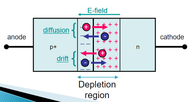
- Equilibrium: diffusion of majority carriers, forming depletion region with E (
) that cause drift that balance diffusion
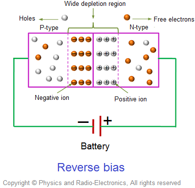
- Reverse bias: temperature dependent, V independent, drift current
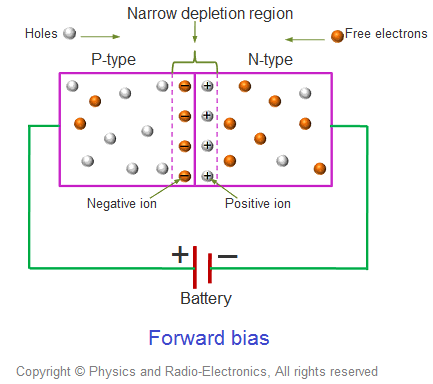
- Forward bias: V dependent, diffusion current
- Reverse Bias: Capacitors, Forward Bias: Diodes
Small signal
- Resistance:
- Capacitance:
- Depletion:
- Diffusion:
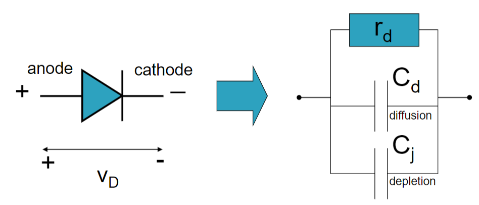
- Depletion:
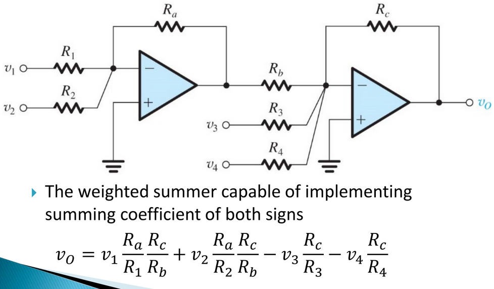
Op-Amps
Topic: Operational Amplifiers
Inverting
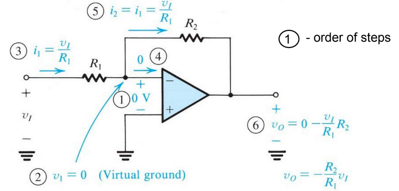
- Ideal:
and
Non-Inverting
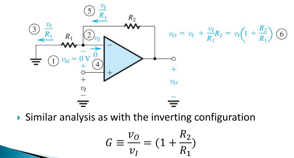
- Ideal:
and
Voltage follower where no resistances on Non-inverting → Amplify Current while keeping the voltage the same.
Difference Amplifiers
Topic: Differential Amplifiers
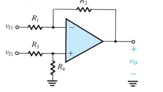
Difference
Common Mode
Diodes
Topic: Semiconductors and PN Junctions
Bias analysis:
V source = SC
Capacitors = OC
Small Signal Analysis:
I source = OC
V source = SC
Capacitors = SC
Inductance = OC
Diodes = R
- Primary goal to analyze diode circuits and precision rectifier.
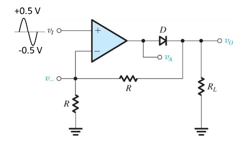
- full wave (bridge) and precision rectifier:
and respectively when - half wave rectifier:
MOSFET/MOST
Topic: MOSFET
When we say for example
- Saturation: Fully Turned, behaves as a voltage controlled current source. When Vds > Vov (Vov=Vgs-Vt)
- Triode: Partially turned on, behaves as voltage controlled resistor. When Vds < Vov.
- For P-Channel just use absolute brackets ||.
- Application of voltage onto the Body of MOSFET → can modulated the channel width, as it changes
.
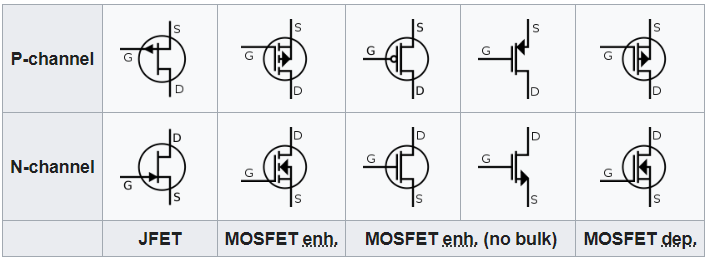
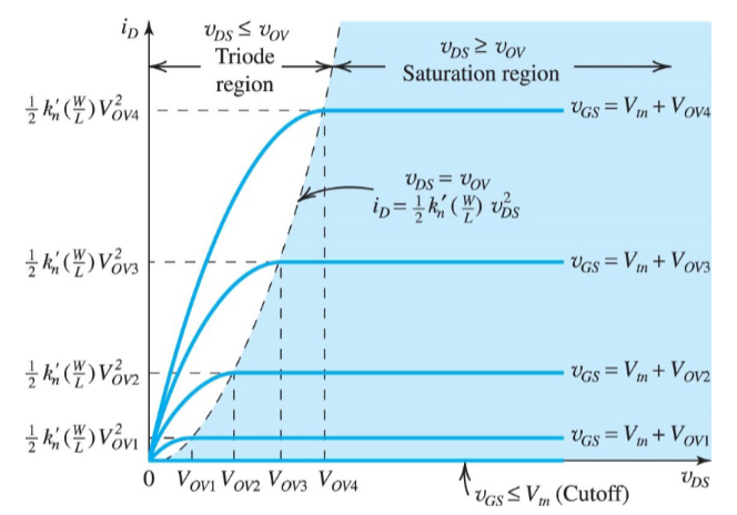
Small
Conductance:
: mobility
: oxide capacitance
: process trans-conductance parameter
W, L: width, length of MOST
: overdrive voltage
→ Voltage controlled resistor with small
Tapered channel
Triode:
- Voltage controlled Resistor
edge of saturation
Saturation:
-Voltage controlled Current source
Channel length modulation:
@
(early voltage):
Output resistance:
Body effect:
Amplifier
Topic: Transistor Amplifiers
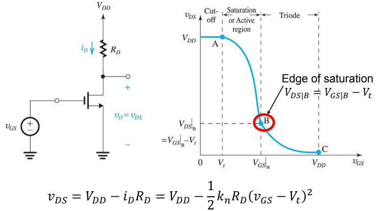
Channel-length modulation:
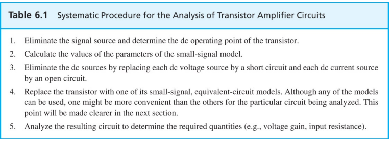
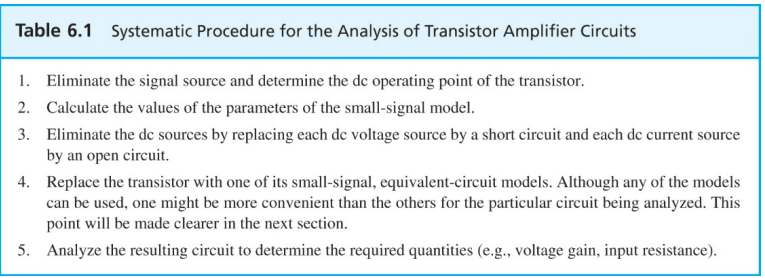
Small signal model:
- V source: SC
- I source: OC
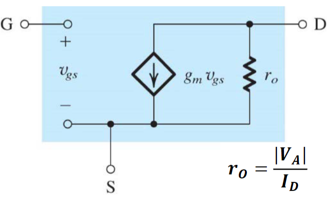
Hybrid-
T model:
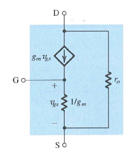
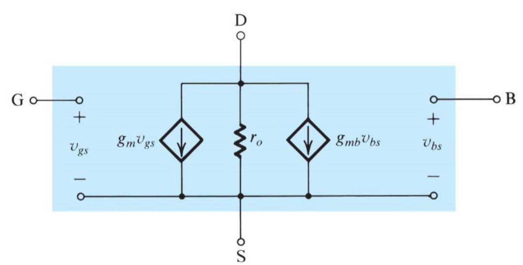
Body effect:
Maximum
Input resistance:
Configurations
Topic: Transistor Amplifiers
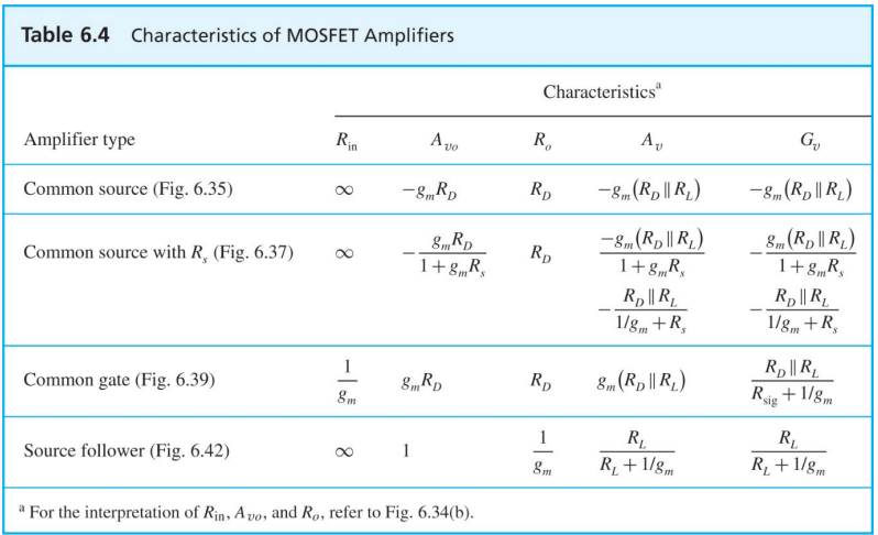
Common source:
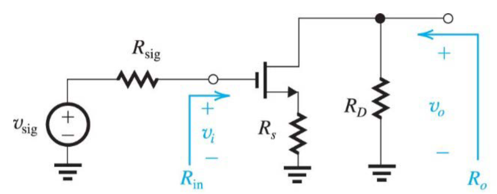
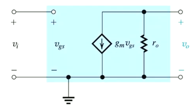
Gain:
Add
Ideal gain:
- Very high/inf
, high - High V gain
- Add CD for low
Common gate:
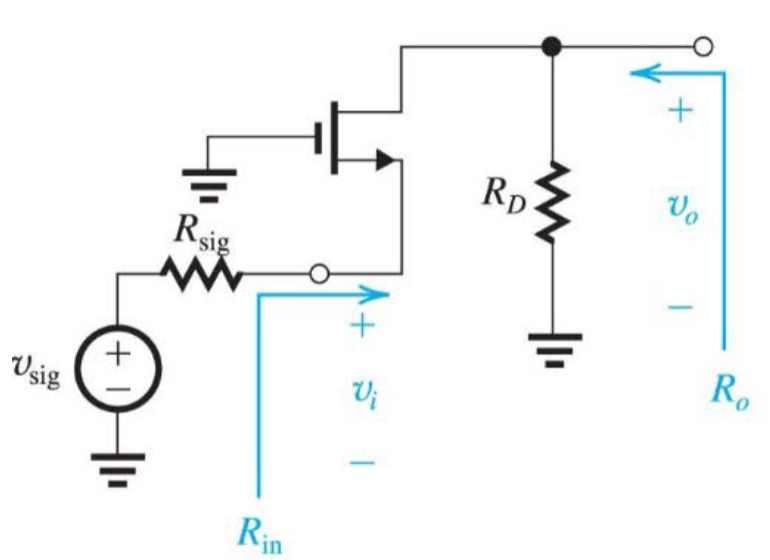
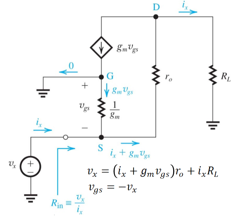
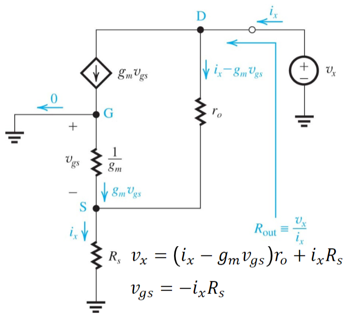
Ideal:
Real:
- Low, controllable
impedance matching with low impedance sources (cables…) >< Input severely attenuated - High
cascode amp
Common drain (source follower)
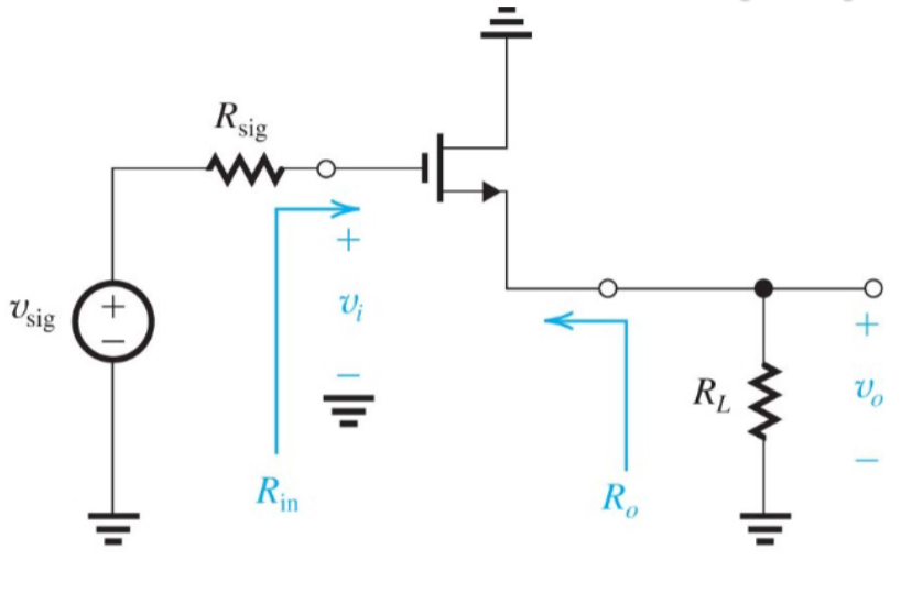
- Very high, inf
, low, controllable - ~1 gain
- Last stage for low
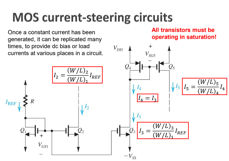
Current steering
Topic: Current Mirrors
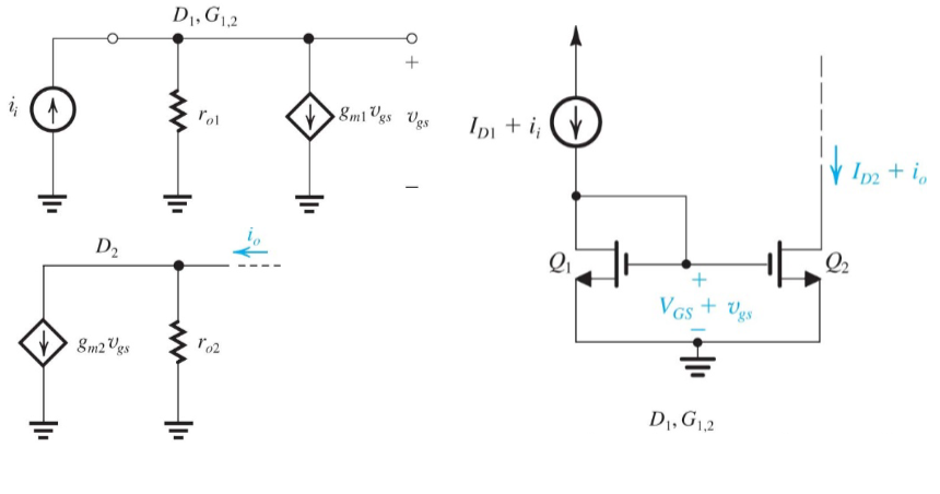
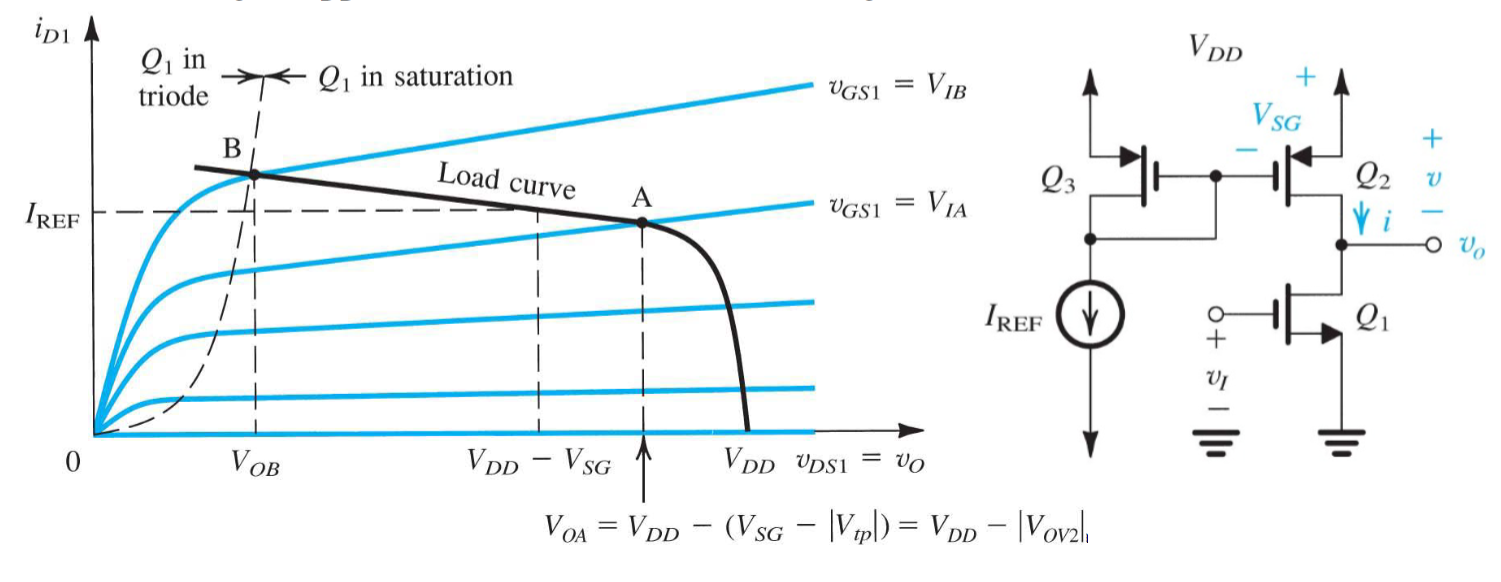
Load curve: I-V of Q2 (
When MOSFETS (identical W/L)→Current Mirror:
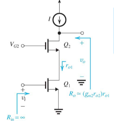
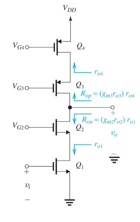
Cascode (CG + CS):
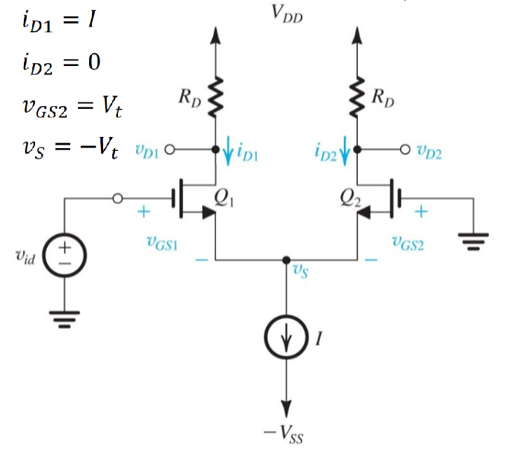
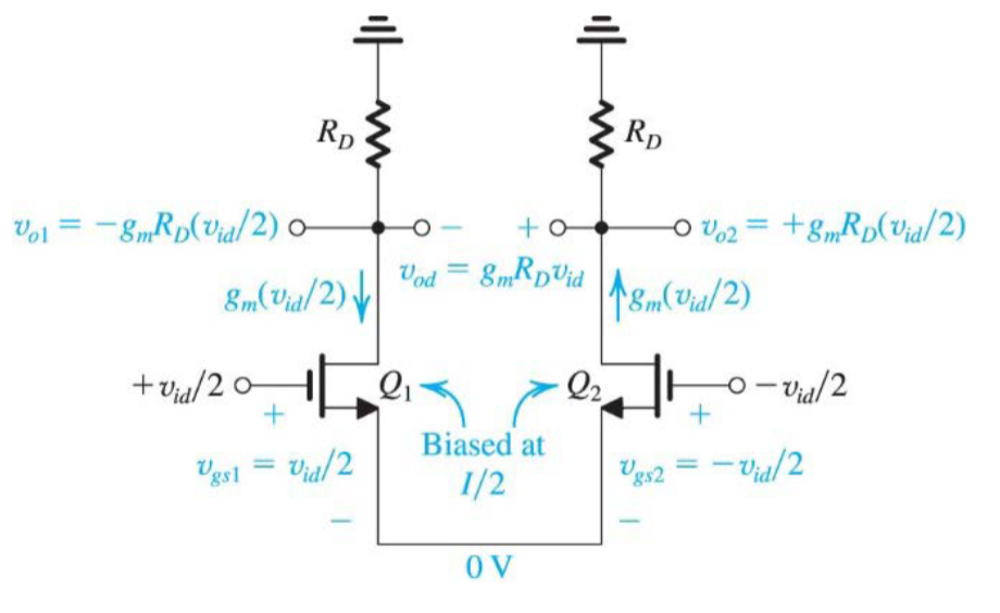
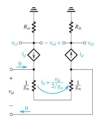
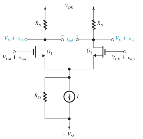
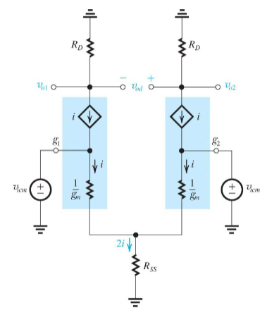
Common mode:
Differential mode:
Virtual GND is established at D → no bypass C to GND in SSA
→ Current source:
CMRR:
Summary for EC2
Limiters
Topic: Oscillators and Waveform Generators
[!NOTE] (Passive) Limiter Circuits
amplitude dependent gain
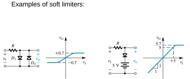
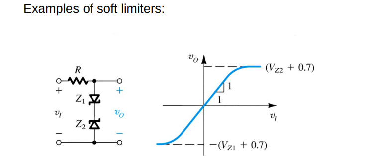
Hard Limiter (clipper): higher amplitude → higher attenuation → distortion
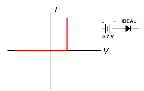
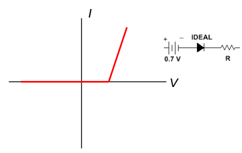
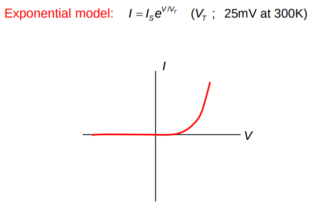
Soft Limiter: less distortion:
- (ideal diode),
- (ideal diode with voltage source (0.7V))
- (ideal diode with voltage source and resistor)
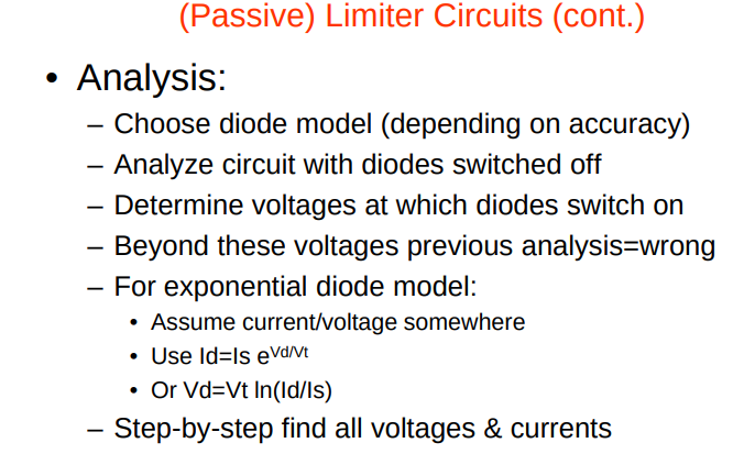
- exponential model:
where at
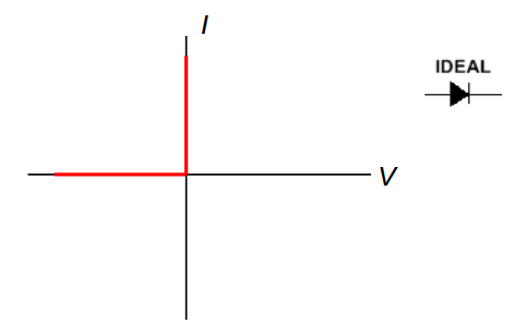
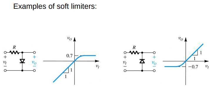
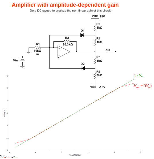
when D2-ON:
when D2-OFF:
Transistors Config
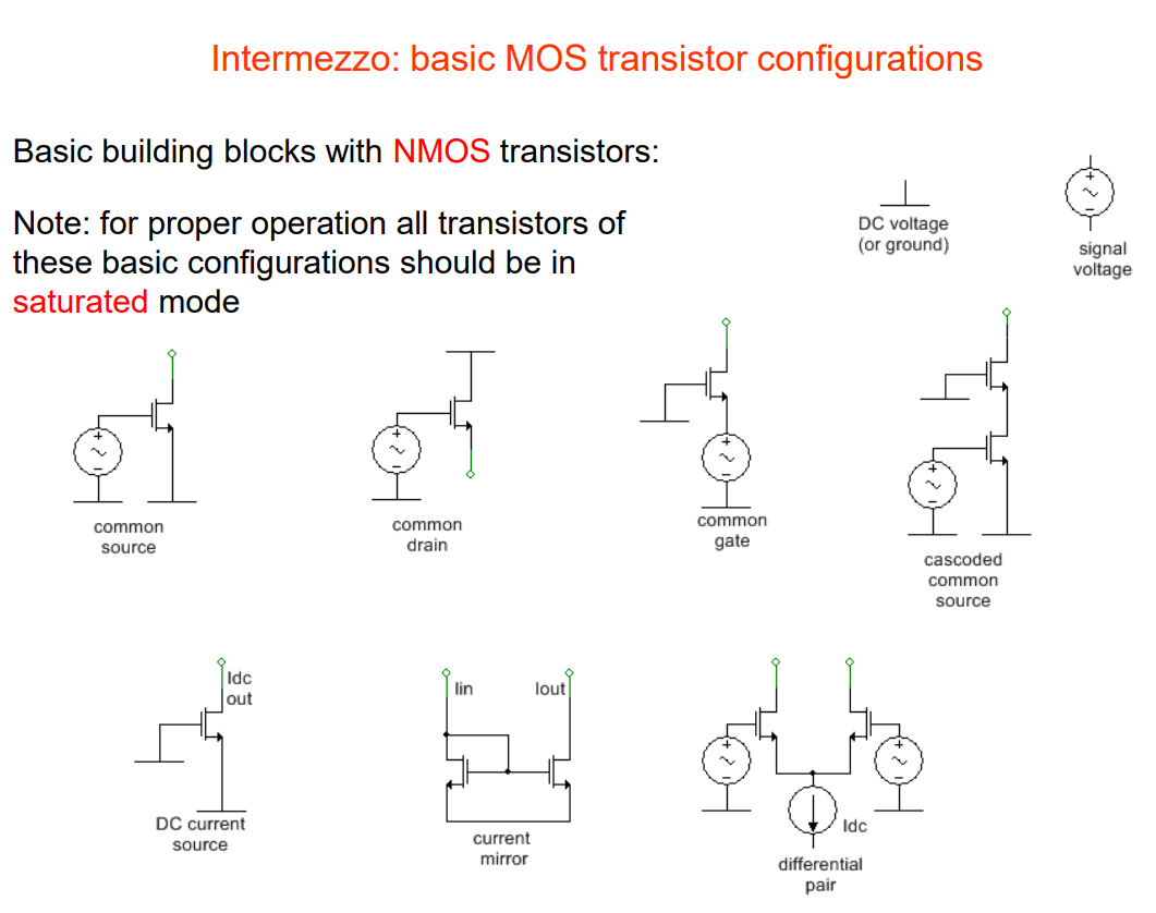
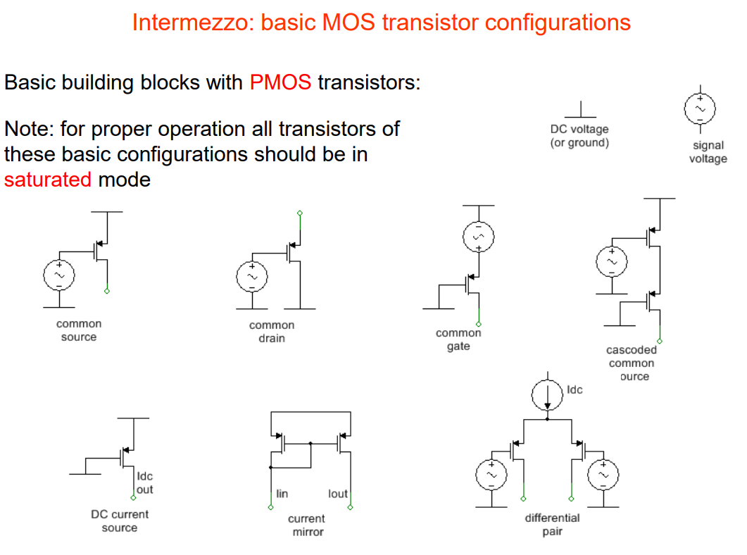
example: common source: means signal enters ground and exits drain
Diode MOSFET
https://www.youtube.com/watch?v=XO30McD3V8w&t=458s
since drain and gate connected: