5XCC0 Biopotential and Neural Interface Circuits
- Area: Electronics
- Topics: Filters · MOSFET · Operational Amplifiers · Data Converters · Systems Engineering
- Related courses: Electronics II - 5ECC0 · Electronics I - 5ECB0 · Electronic Systems Engineering - 5XIC0
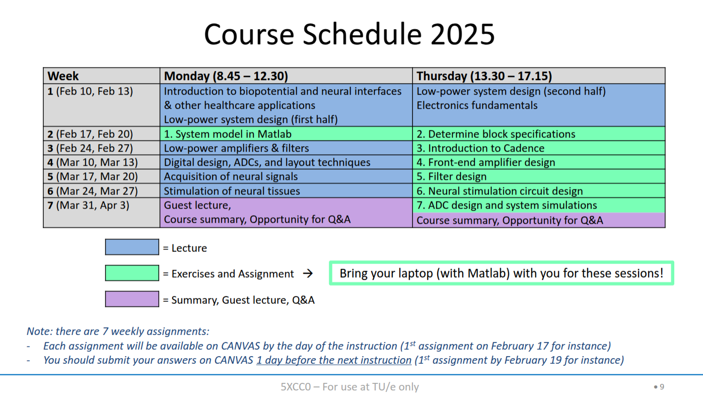
Schedule
Health Applications
5XCC0-01 Health Applications.pdf
Formulas
Electrode Capacitance
Impedance of a Capacitor
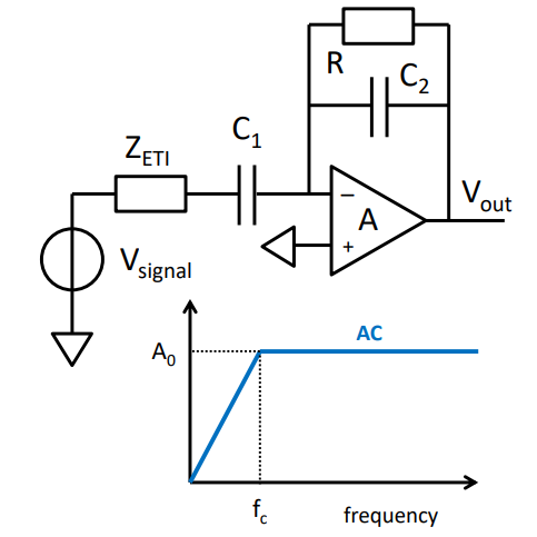
Amplifier Gain (AC Coupling)
Cut-off Frequency (AC Coupling)
Input Impedance (Capacitive)
Signal Attenuation due to Impedance
CMRR (Common-Mode Rejection Ratio)
CMRR due to Electrode Mismatch (Approx.)
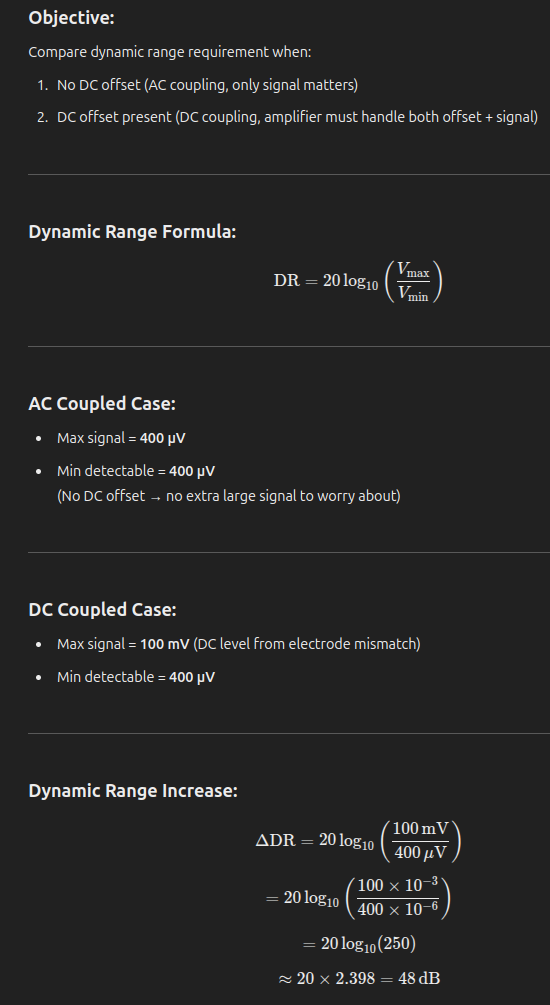
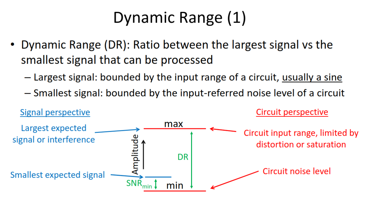
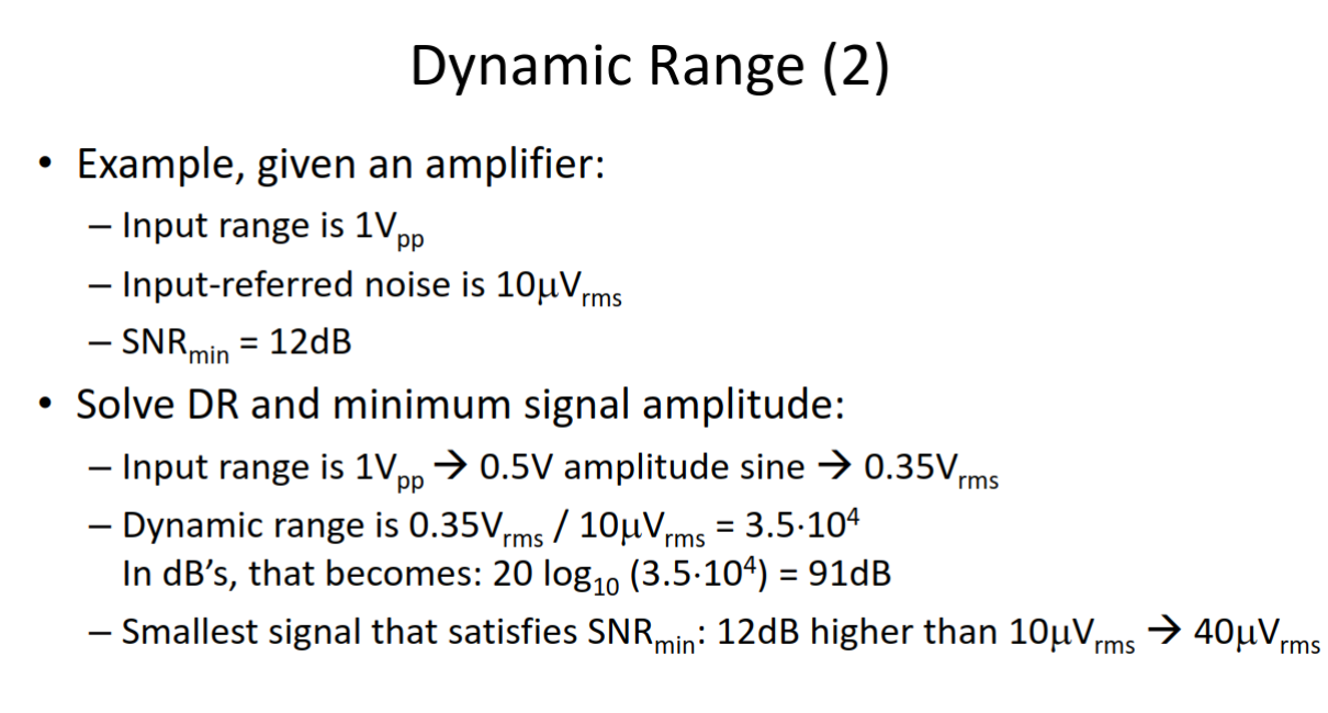
Dynamic Range
1/f Noise Trend
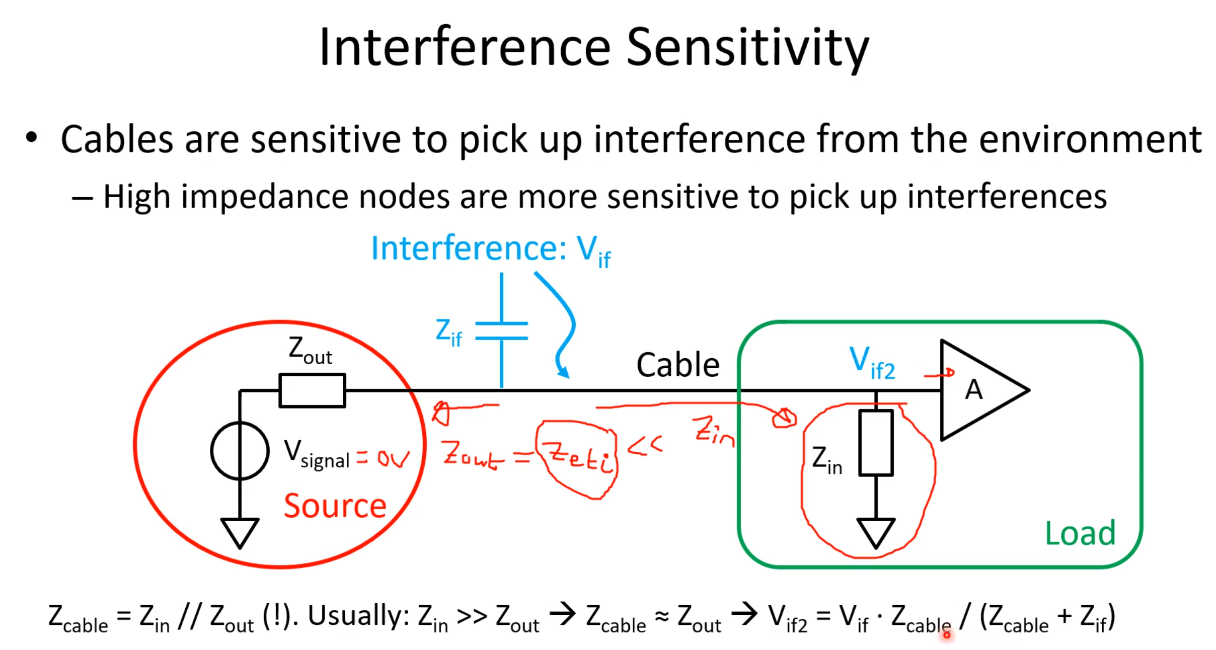
Voltage Divider for Interference Sensitivity
Transfer Function for Capacitive Coupling Interference
IRN
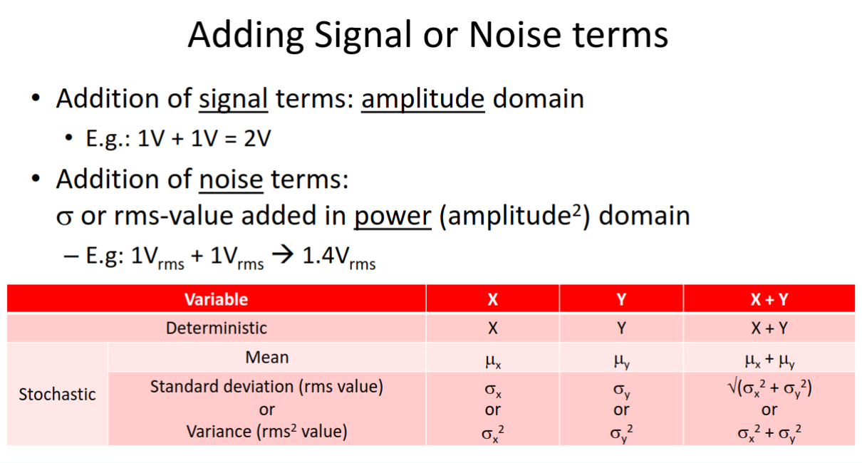
Adding them in RMS:After amplifier the filter and ADC see factor of 10 from amplifier.
Other
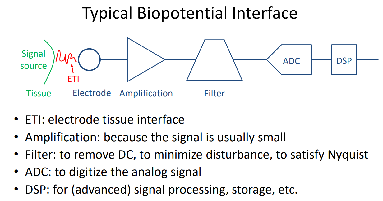
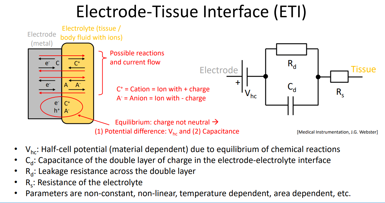
Electrode types
Gel: galvanic connection: lowest and reliable impedance → skin prep.
Dry: higher less reliable impedance → no skin prep
Capacitive: galvanic isolated electrode (capacitive coupling): highest impedance but best comfort.
Measurement challenges: small signal amplitudes, large ETI impedances, large disturbances, close to DC information needed

Dealing with small signal: high gain required for amplification, since the signal of interest is usually (
- Minimum signal amplitude should be detectable by the system. (at ADC).
- Maximum signal, interference, DC, etc., should not saturate the system.

- electronics add random noise (thermal noise, 1/f noise, quantization noise).
- ETI, environment and tissue add noise.
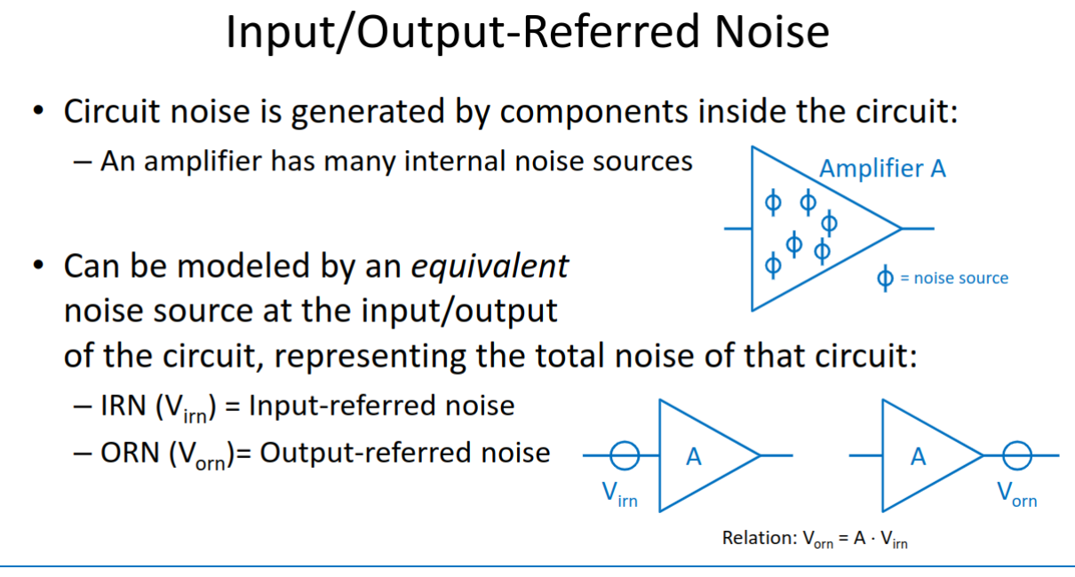
- IRN (input-referred noise): sensitivity of system: should be smaller than smallest signal you want to detect.
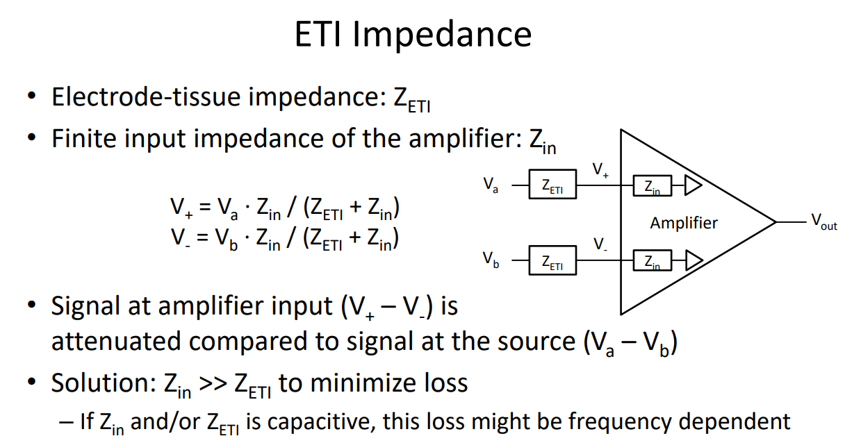
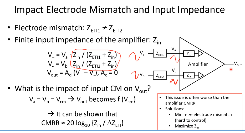
ETI Impedance:
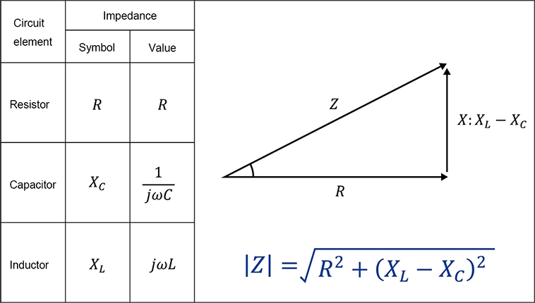
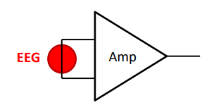
maximizing without saturation of amplifier (accounting for interference and disturbances):
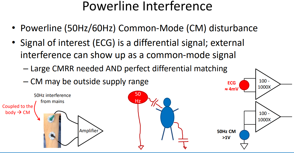
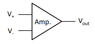
Common-mode Rejection Ratio (CMRR):
There are various (slight) differences in CMRR definitions.
CMRR looks at small signal behavior. If CM disturbance is large, amplifier might saturate, and the small signal model does not hold.
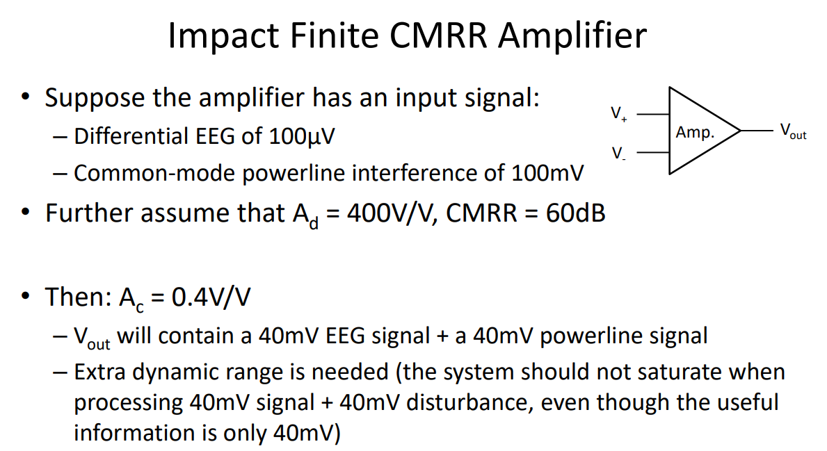
EEG signal (differential):
Power-line interference (common-mode):
So we need enough dynamic range to accommodate both the signal/disturbance without saturation.
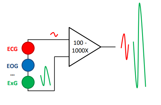
large dynamic range needed, spatial discrimination, frequency-domain filtering, time selection, advanced dsp.
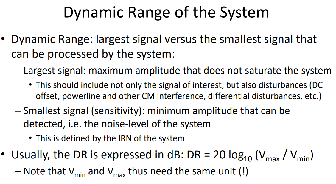
dynamic range:
CMRR to Common-Mode Gain - Multiple differential contibutions
common-mode interference:
and CMRR given.
eg:
since we care about input voltage contribution we don’t need exact gain values.
CM suppression factor = 1000
ifthen if we have multiple differential contributions like EEG signal, disturbance signal, converted CM interference:
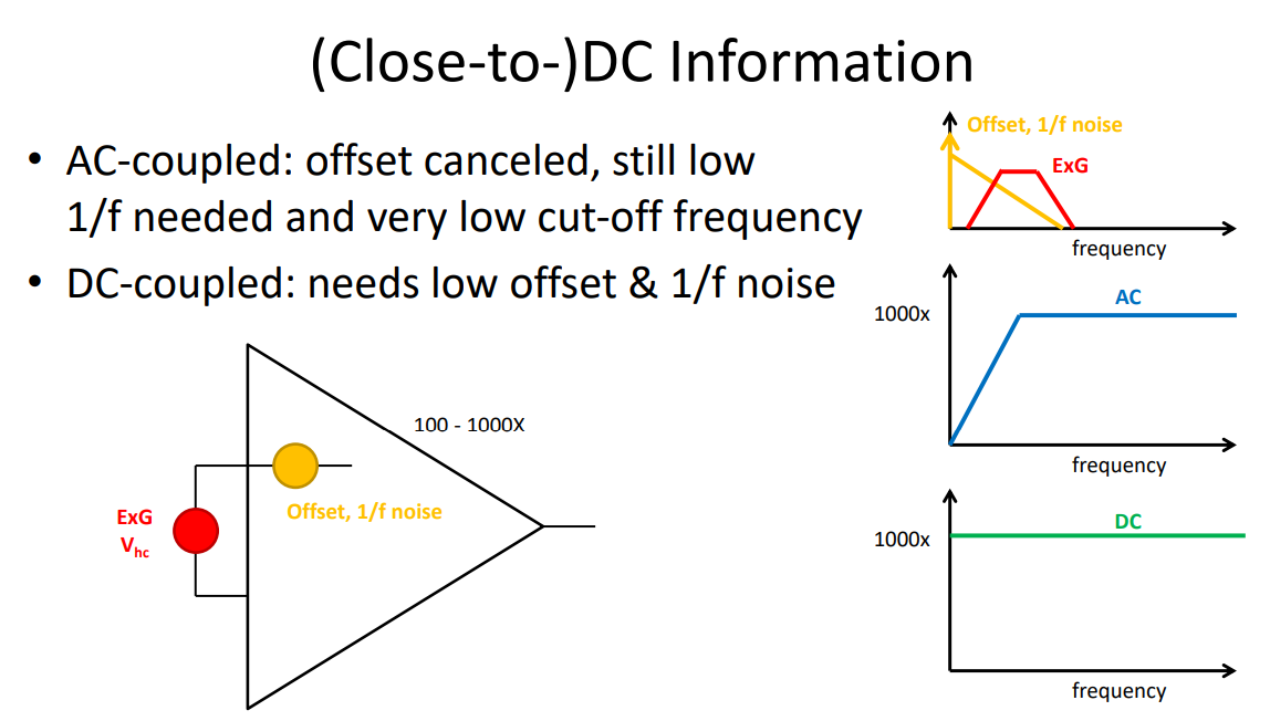
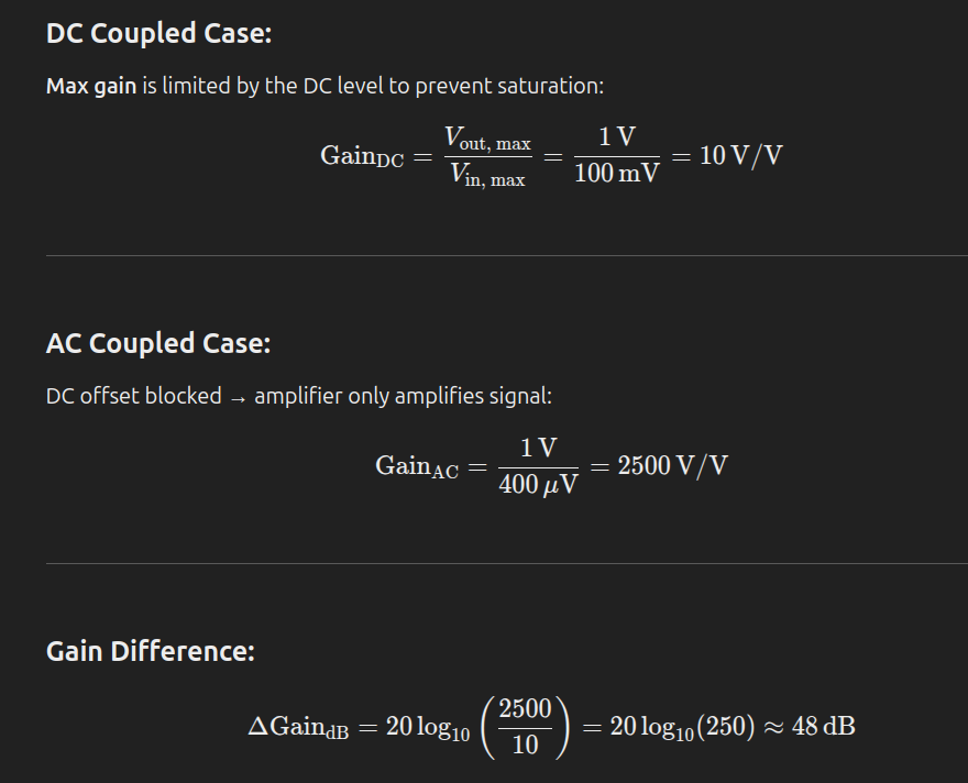
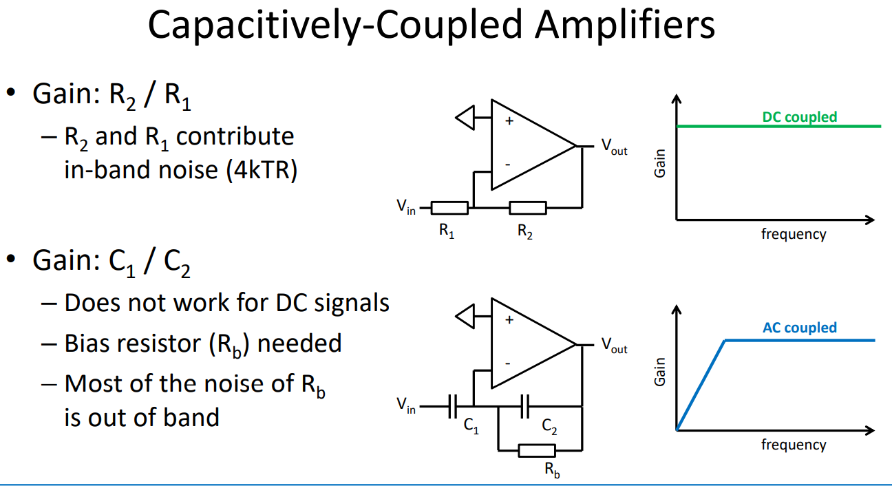
AC coupling & DC Coupling
AC coupling should be before amplification, otherwise saturation:
- Gain:
- Cut-off frequency:
signal attenuation:Trade-off:
- For large
small - For low
, high gain large
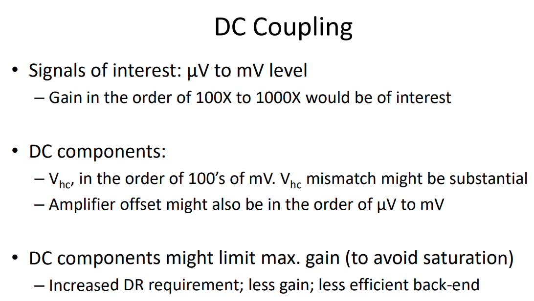
Assume we have a DC coupled amplifier. Due to electrode mismatch, the half-cell potentials result in a differential DC level of up to 100mV. The signal of interest is 400µV. The amplifier has a 1V output range.
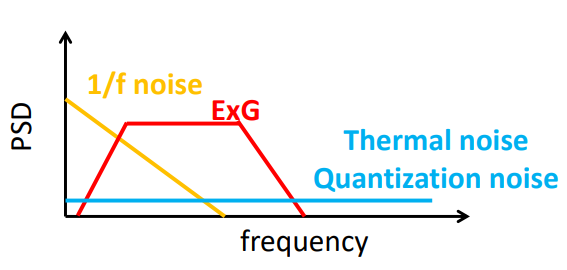
- 1/f noise (flicker noise) has a power-spectral density (PSD) that is inversely proportional to the frequency
- ExG signals are at low frequencies too
- Often the 1/f noise is dominant compared to white noise sources
Can look at slides for example details of health applications
Low-Power System Design
Summary
5XCC0-02 Low-Power System Design.pdf
Formulas
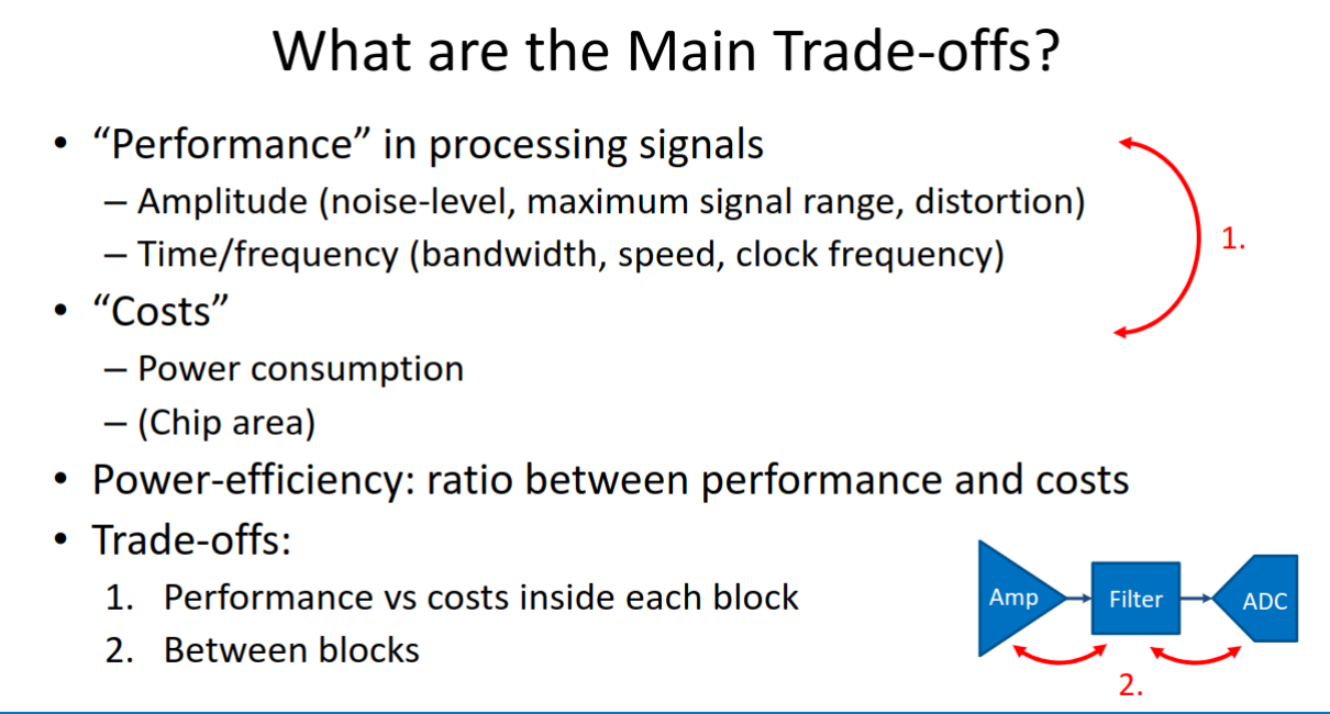
Power vs bandwidth and noise for analog (amp):
Noise Efficiency Factor (NEF):
Power vs DR for ADC (mixed-signal):
Schreier Figure of Merit (FOMS):
Dynamic Range (general):
DR due to quantization (digital):
Effective Number of Bits (ENOB):
Quantization noise (uniform distribution):
Input/Output referred noise:
Total input-referred noise (cascaded blocks):
Input-referred quantization noise (ADC):
FOMS estimation rearrangement:
Least significant bit
RMS→
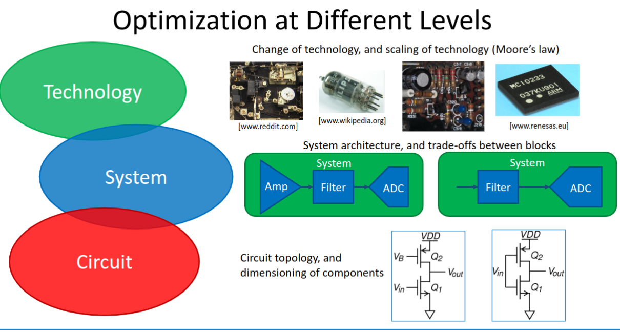
V model, Risk, Optimization
Topic: Systems Engineering
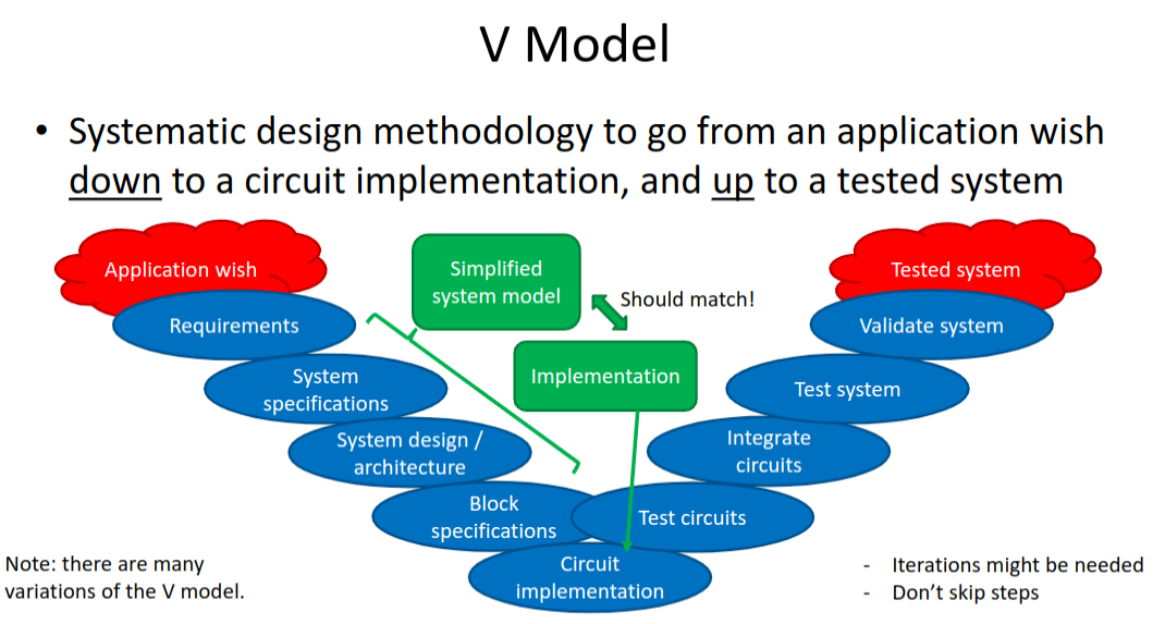
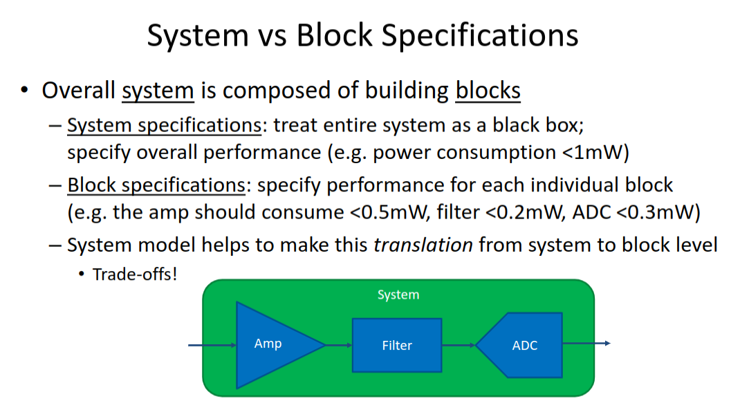
requirements: what can product do.
specification: how design meet requirements.
verification: whether circuits/blocks system meet specifications/requirements.
validation: overall solution meets needs.
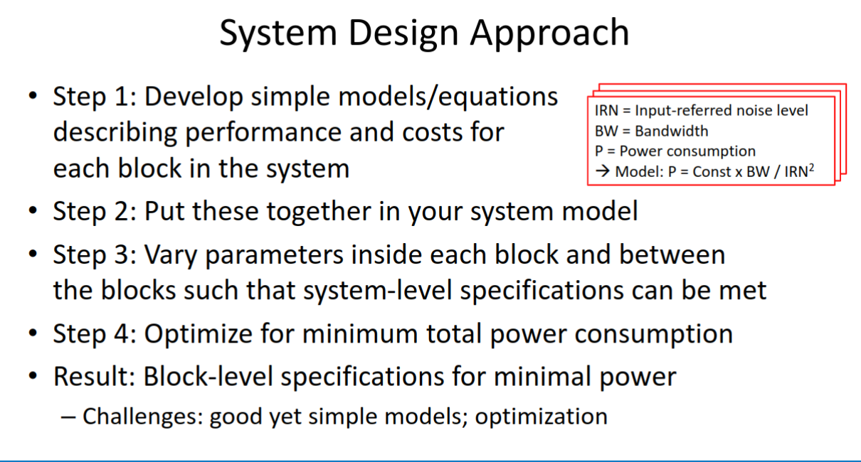
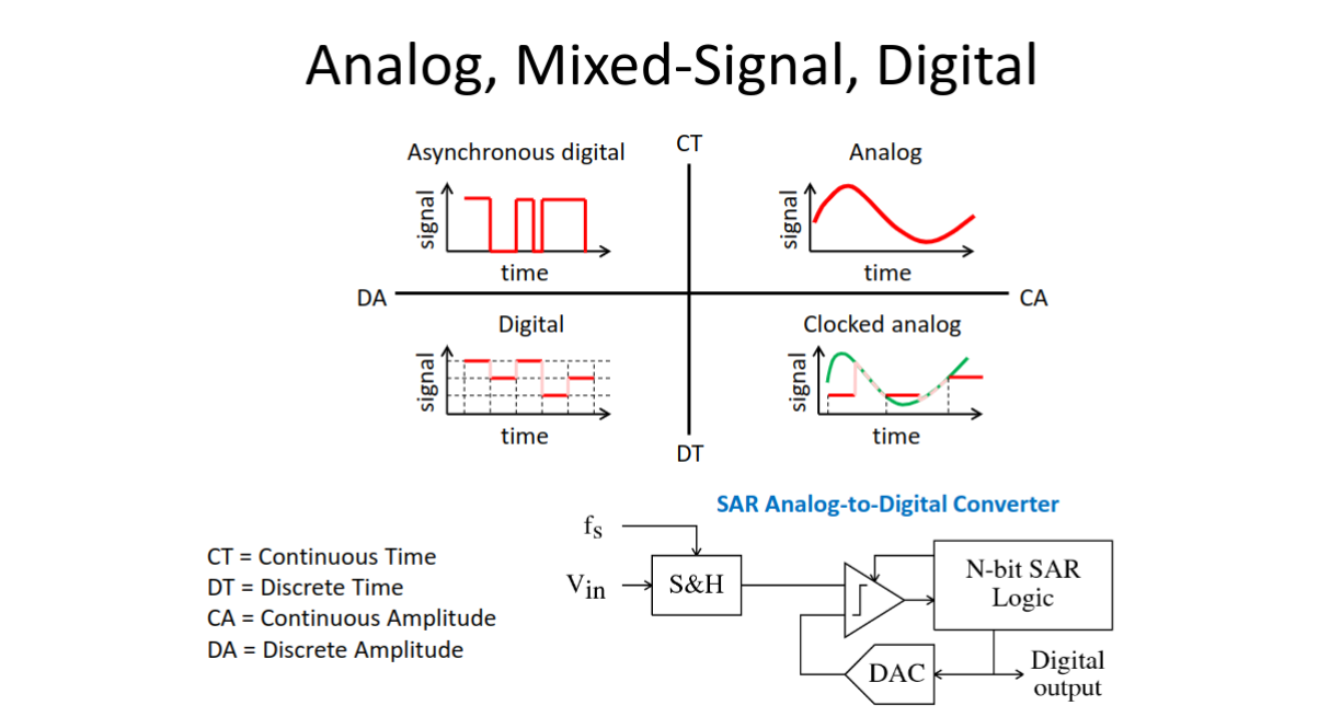
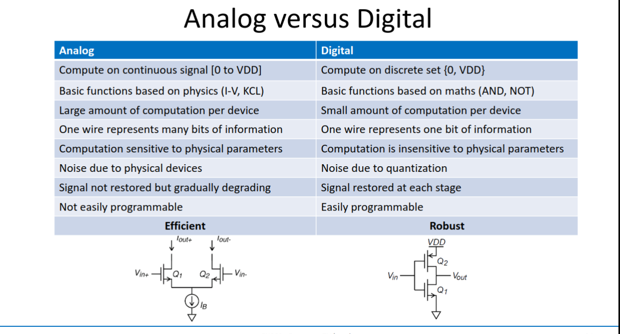
Analog, mixed-signal, and digital circuits
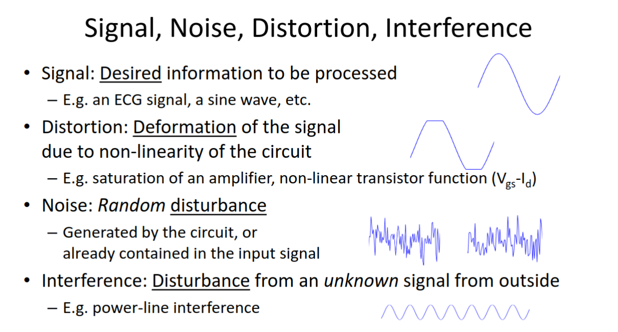
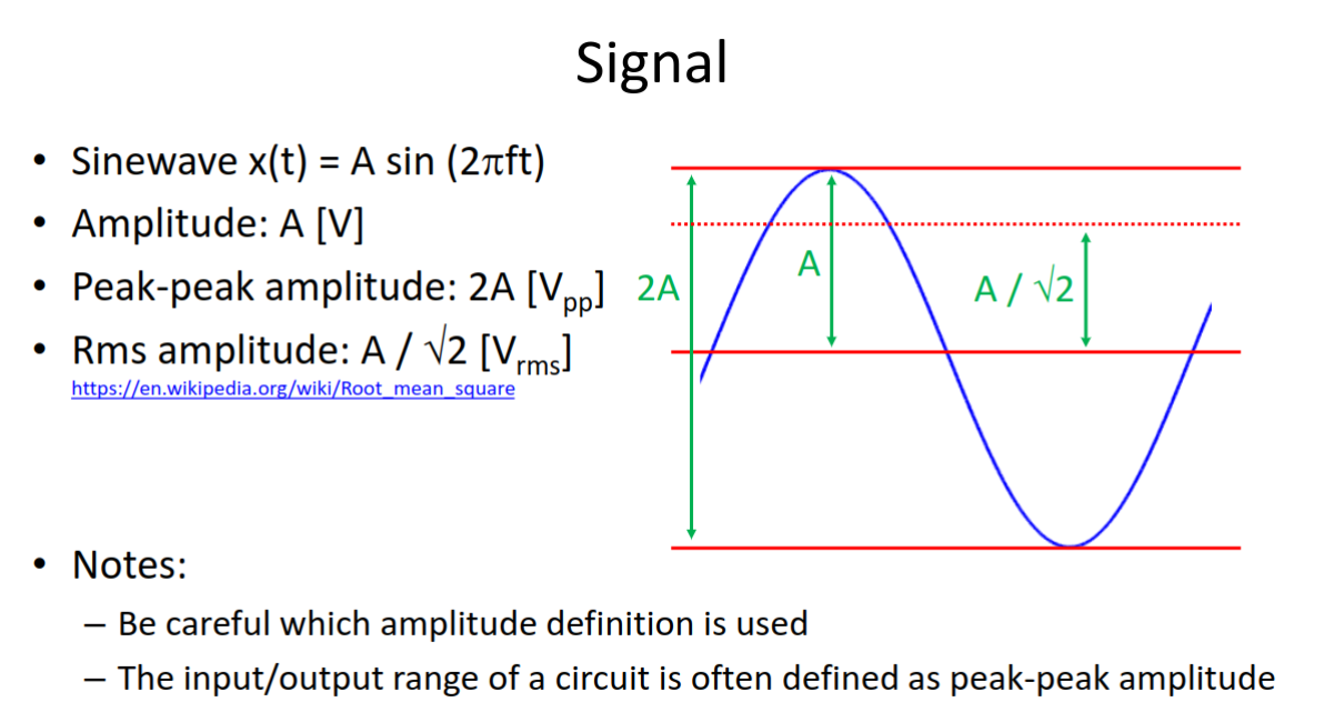
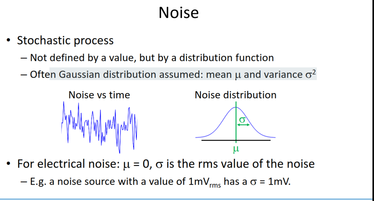
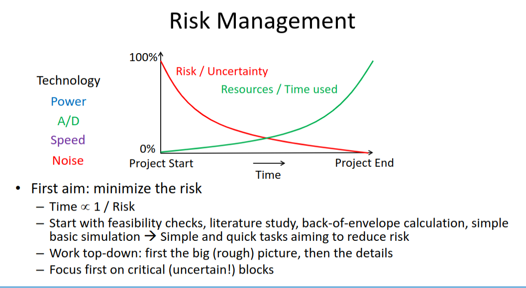
System Analysis Example
Signal → Amplifier (gain = 100) → Filter (gain = 1) → ADC
. input range of the system would be the most severe limit:
in this case would be .
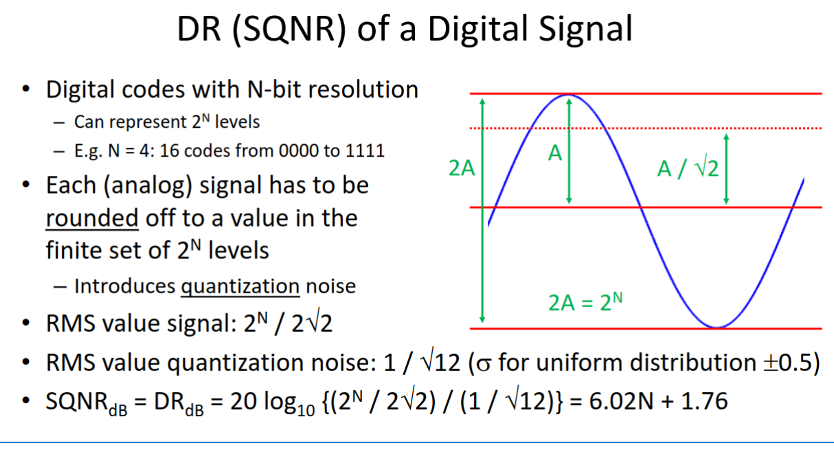
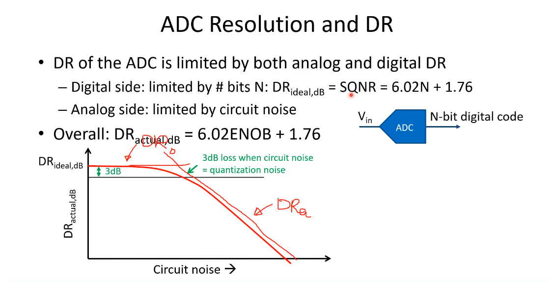
ENOB is the effective number of bits (or effective resolution) including the effects of quantization noise and circuit noise: ideally equal to N, but in practice smaller.
ADC Resolution and DR
levels/codes:gain of ADC from input voltage to output code:
.
where RMS value quantization noise
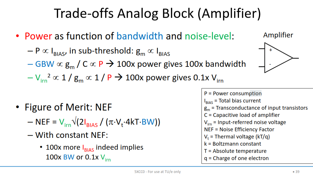
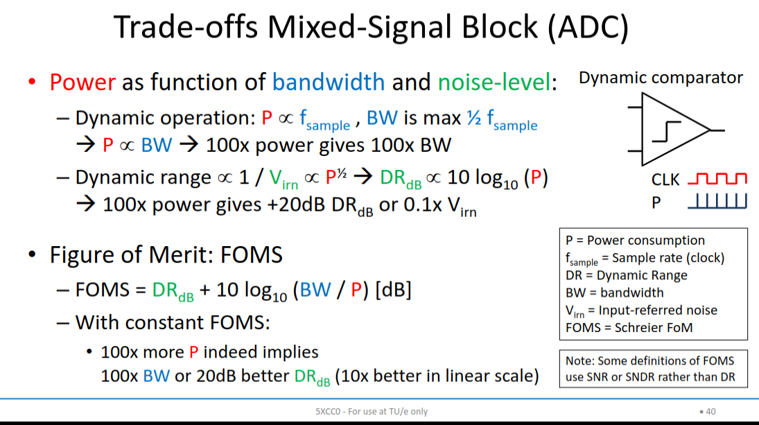
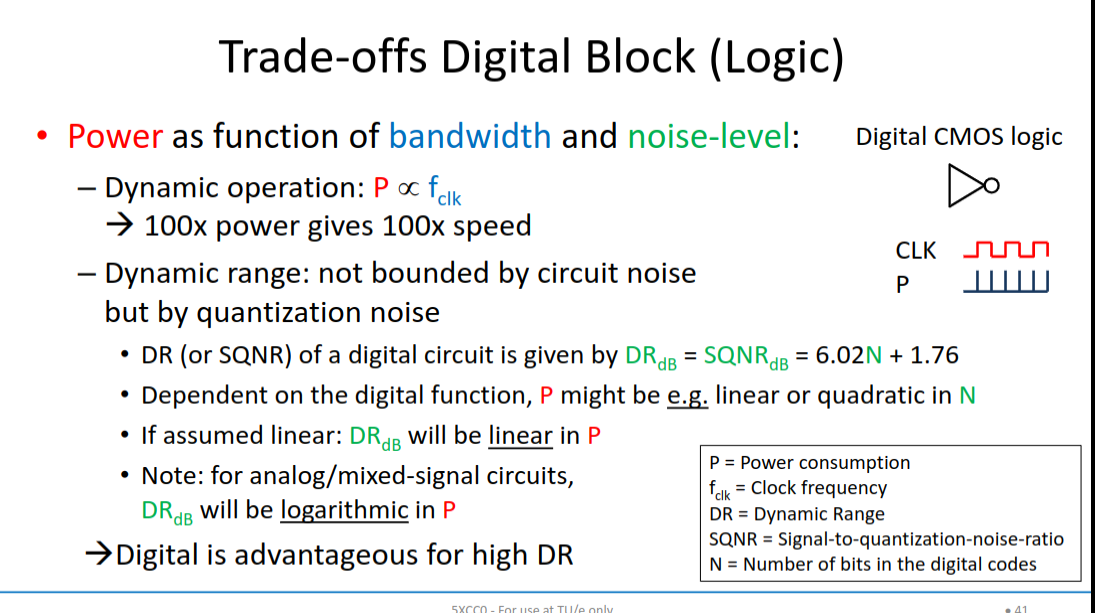
The lower the NEF (closer to unity) the better.
Noise Efficiency Factor (NEF):
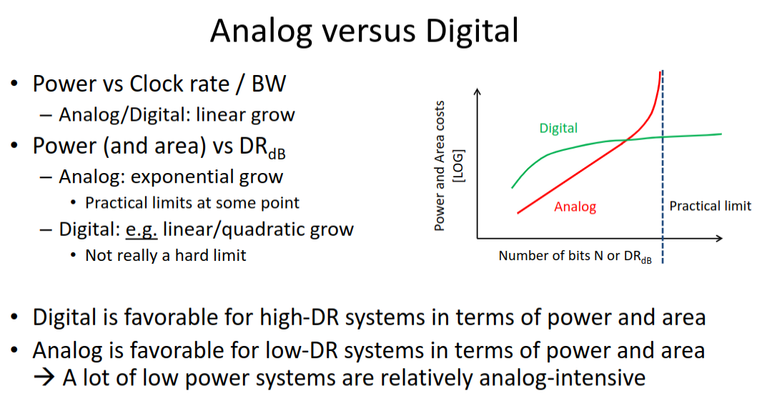
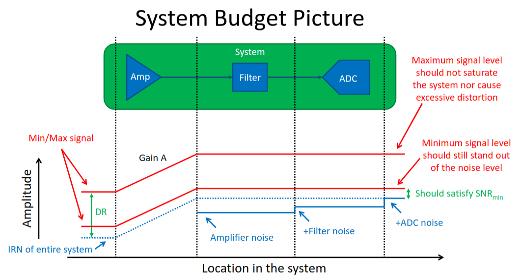
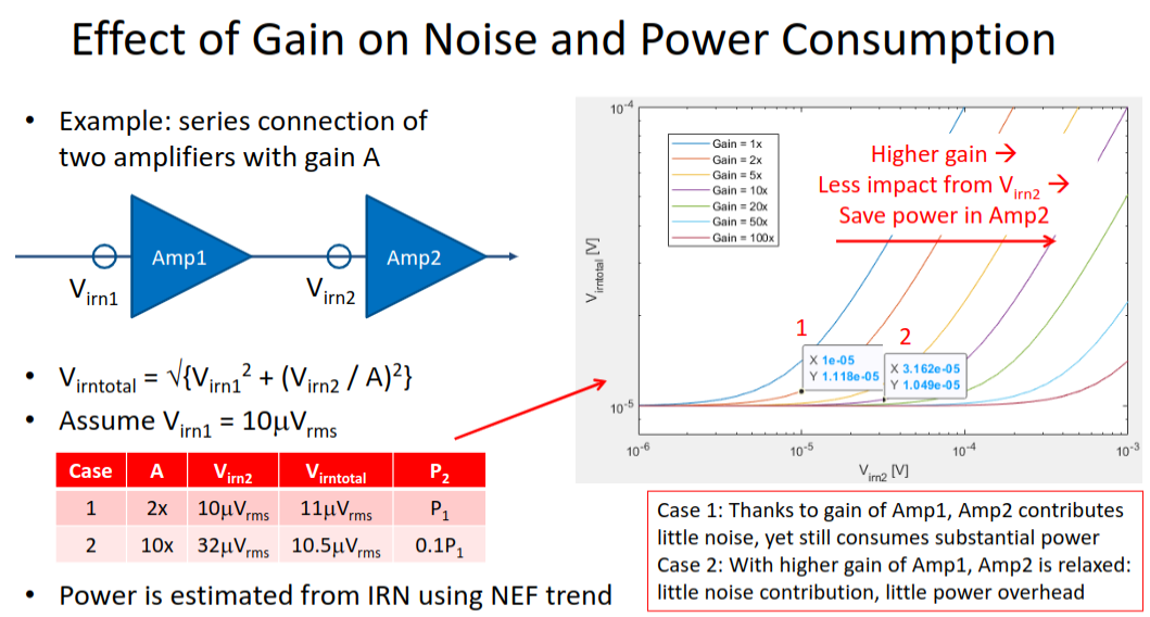
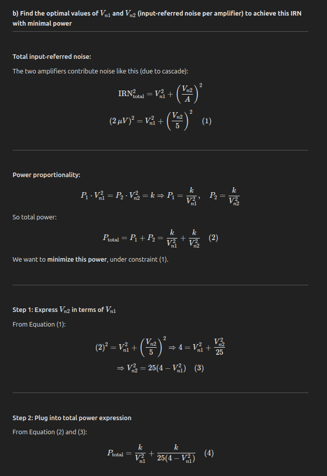
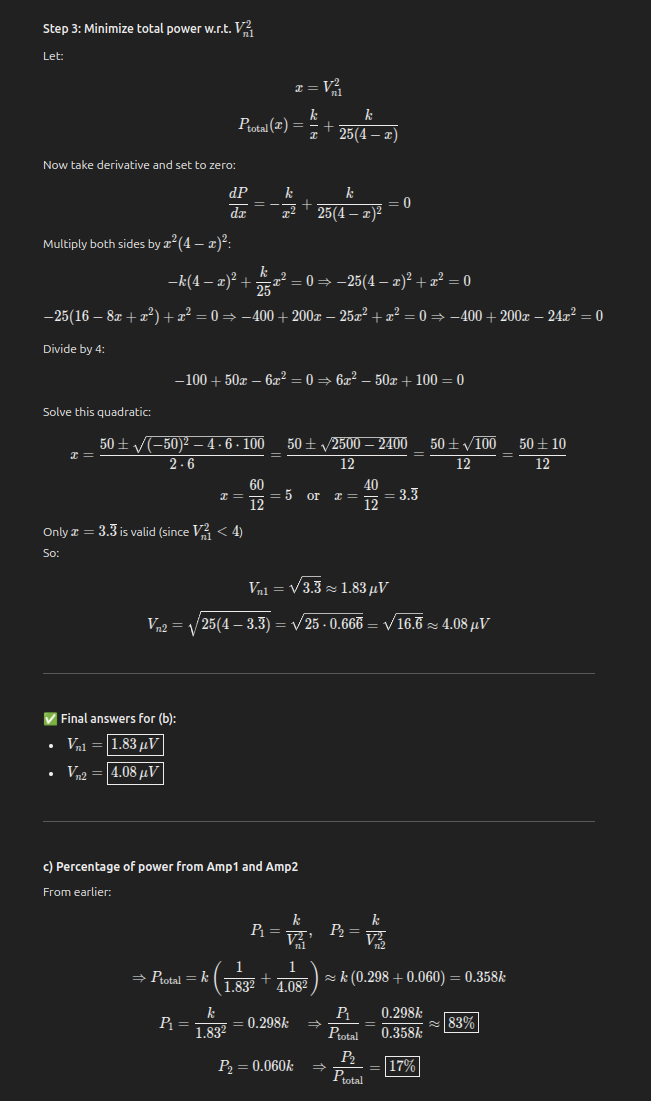
Models of power and performance in amplitude/frequency
Frequency: analog & digital scale similar
Amplitude: analog favorable for low DR, digital favorable for high DR
Electronics Fundamentals
Topic: MOSFET
5XCC0-03 Electronics Fundamentals.pdf
Formulas
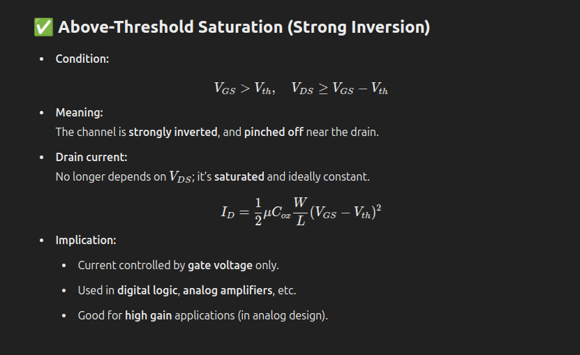
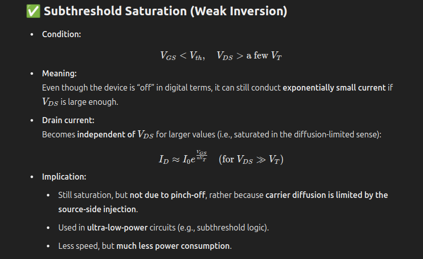
Sub-threshold region (MOSFET):
Above-threshold, Linear mode (MOSFET):
Above-threshold, Saturation mode (MOSFET):
Thermal voltage:
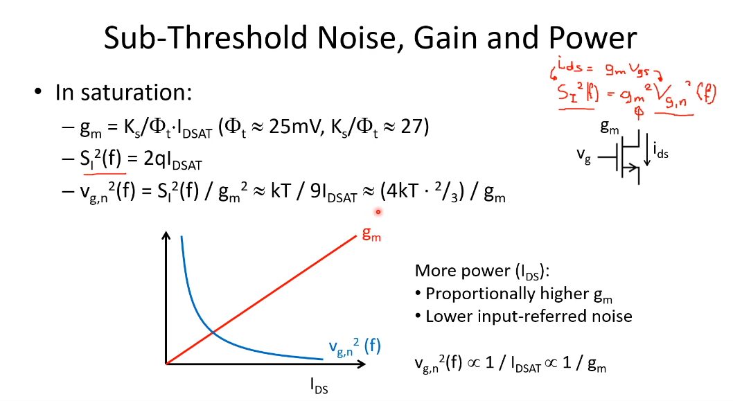
Transconductance (gm):
Sub-threshold:
Above-threshold:
Efficiency ratio:
Sub-threshold:
Above-threshold:
Shot noise (current):
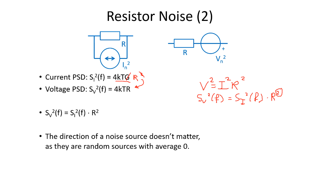
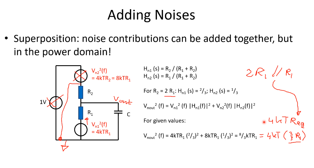
Thermal noise (resistor):
Current PSD:
Voltage PSD:
Noise power (bandwidth
):
Current noise:
Voltage noise:
Integrated noise amplitude:
Noise at MOS input (sub-threshold):
Noise at MOS input (above-threshold):
1/f noise:
Sub-threshold:
Above-threshold:
General:
Voltage divider ratio:
Effective resistance:
Low-pass filter cutoff frequency:
Sampled noise power (switched capacitor):
SNR (in dB):
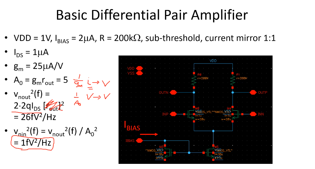
Small signal gain of differential pair:
Noise output of differential amplifier:
Input-referred noise:
other
diffusion current:
drift current:
In saturation the current
- trans-conductance efficiency:
the ration of trans-conductance to drain current, tells how much gain you get per unit of current. Which is power efficiency. - It is constant in sub-threshold → why that mode operation is great for low power electronics.
- Increasing
improves performance in strong inversion mode.
signal power:
noise power spectral density:
total integrated noise power:
Amplifiers and Filters
Topic: Filters
5XCC0-04 Amplifiers and Filters.pdf
Formulas
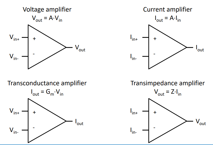
- Voltage amplifier:
- Transconductance amplifier:
- Current amplifier:
- Transimpedance amplifier:
- TIA transfer function (ideal):
- TIA with op-amp gain
: - Transconductance amplifier:
, - Input-referred noise OTA:
- CS voltage amplifier gain:
- Inverter-based voltage amplifier gain:
- Input-referred noise CS VA:
- Input-referred noise INV VA:
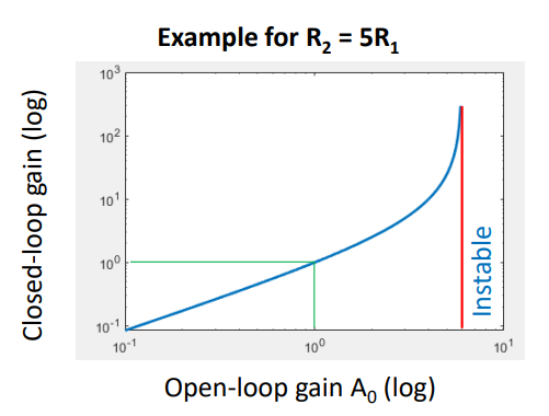
- Positive feedback gain:
- Condition for stability:
- Input impedance with positive feedback:
when - Capacitive amplifier gain:
- Gm-C filter time constant:
- Gm-C 1st-order LPF:
- Gm-C 2nd-order LPF:
- Gm from bias current (subthreshold):
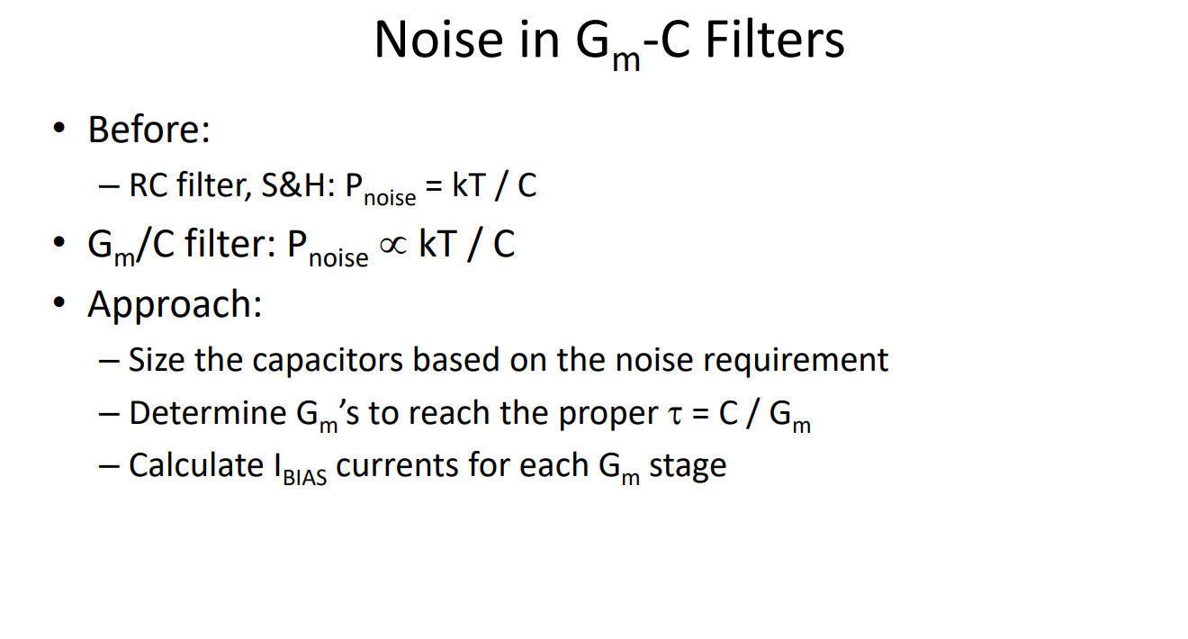
- Noise in Gm-C filters:
Amplifier Types
Topic: Operational Amplifiers
Concepts to be familiar with
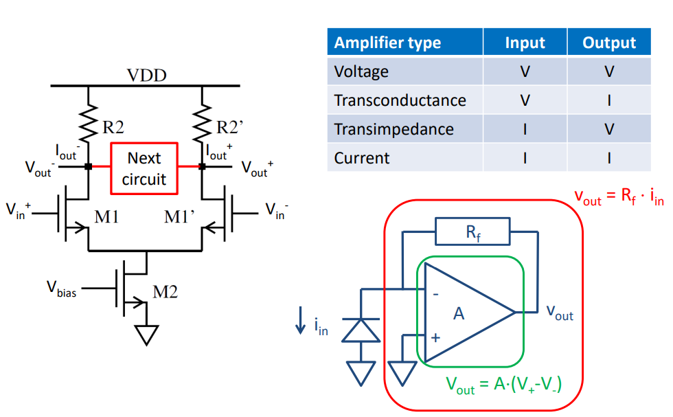
- Differential pair
- Current mirror
- Common-mode, differential-mode
- Common-mode feedback
- Open-loop, closed-loop, stability, phase margin
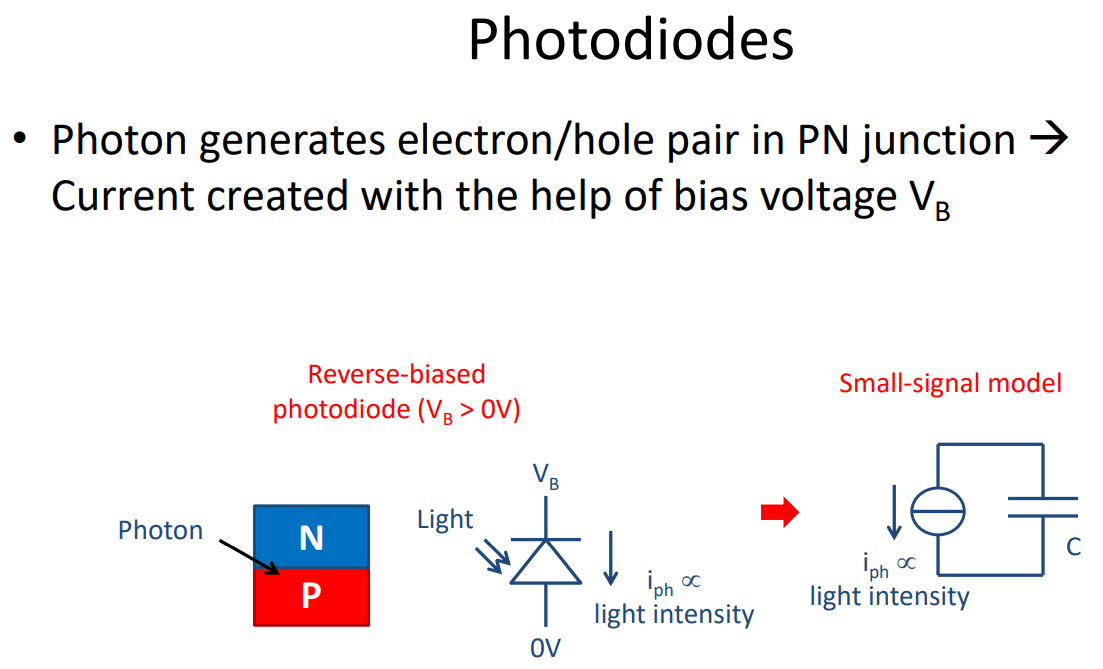
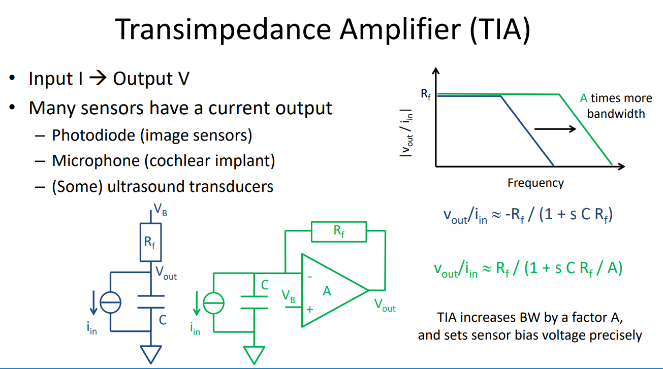
Transimpedance Amplifiers
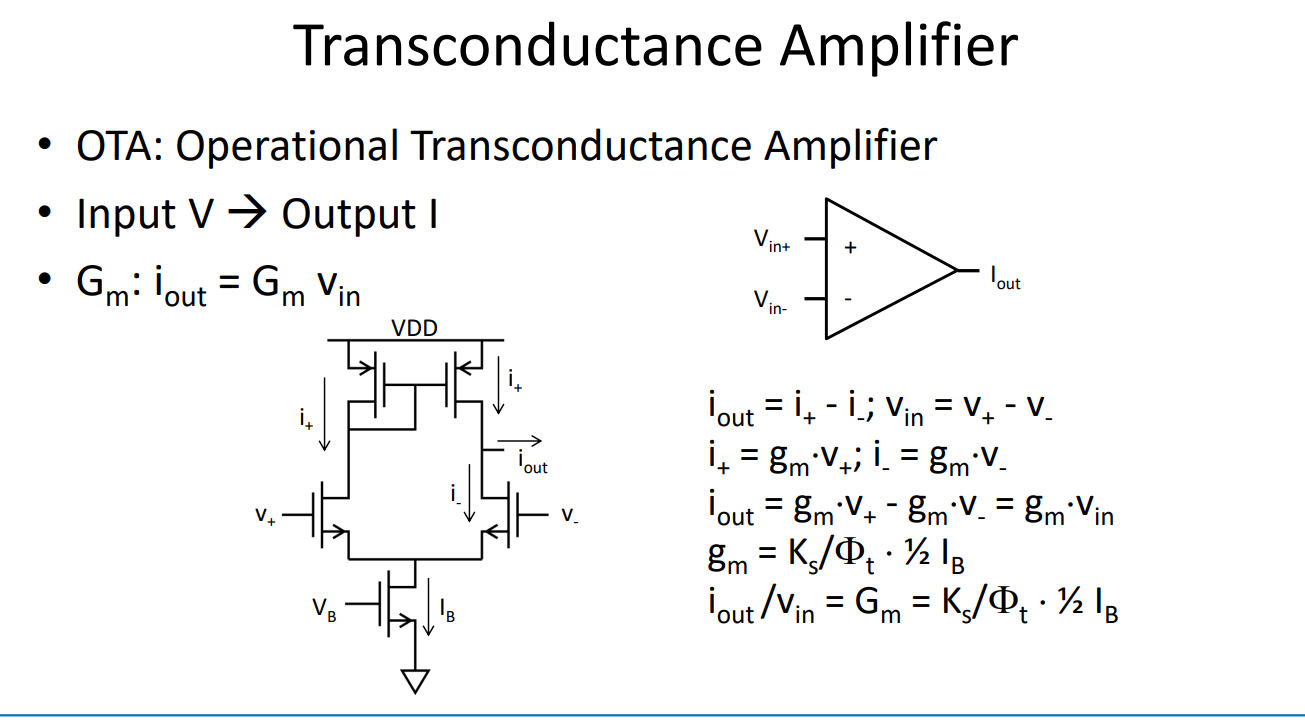
Transconductance Amplifiers
Voltage Amplifiers
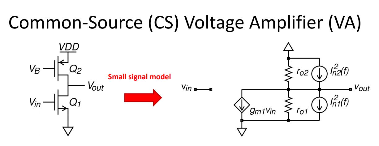
The reason for small signal model not having
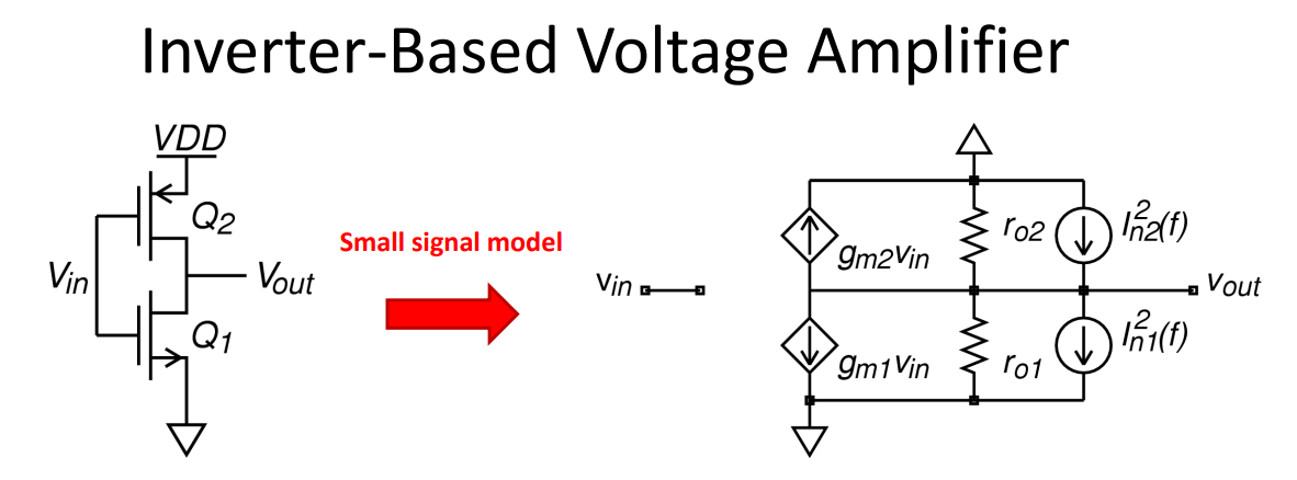
More gain (about 2x) and lower input-referred noise power spectral density (about 4x) compared to CS VA.
Advanced Amplifier Techniques
Low-Voltage Analog Design
- Each transistor needs a certain
- Minimize number of stacked transistors
- Use sub-threshold biasing (lower
) - Use cascaded stages rather than cascoded transistors to increase gain.
- Increase DC gain by positive feedback.
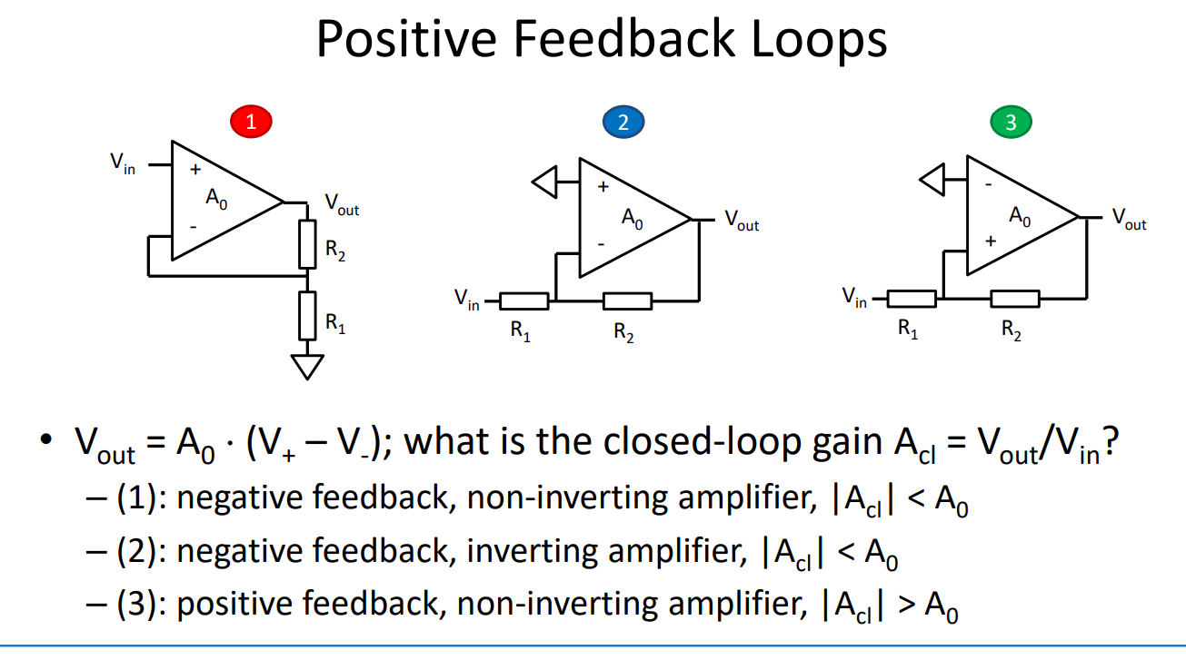
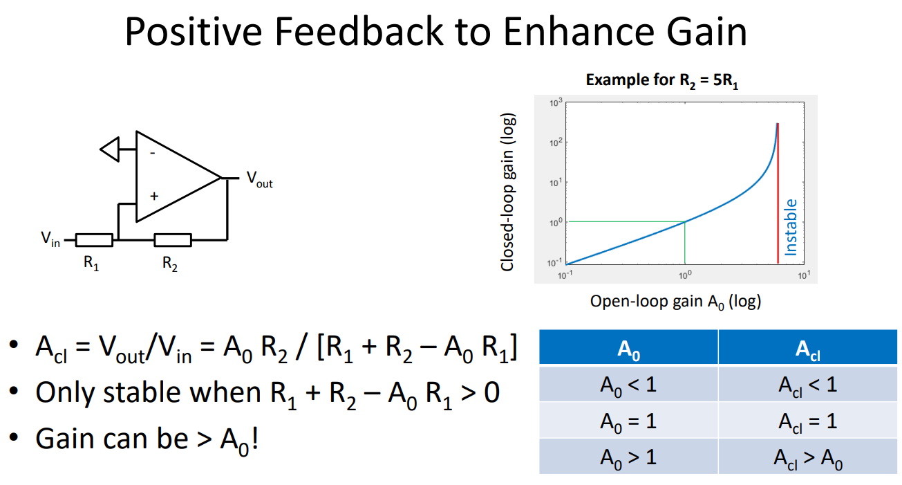
negative feedback:
Positive vs Negative Feedback Amplification
- Positive feedback entails adding the output of a function or process to its input. Negative feedback is subtracted from the input instead of being added.
- The effect, generally, is that positive feedback causes the output, or its amplitude, to grow without bound or until a saturation level is reached.
- Another purpose for positive amplification is to enhance impedance. So either increase gain or enhance impedance.
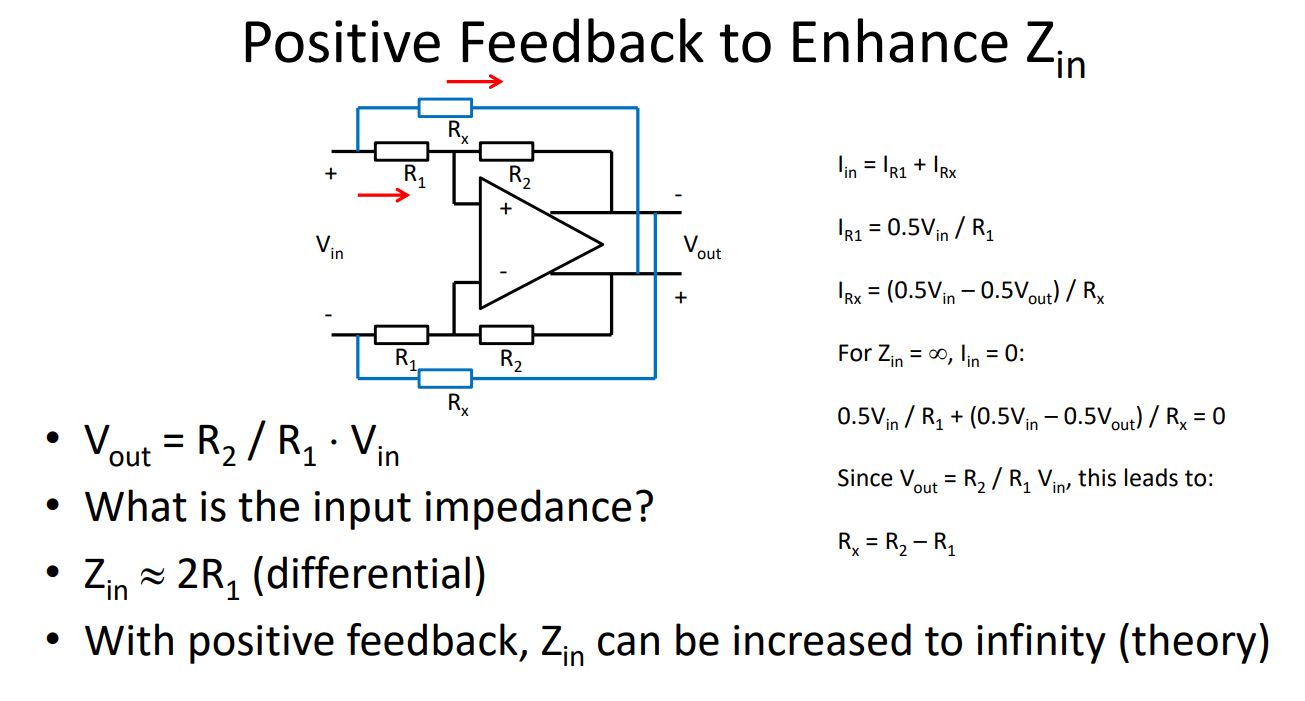
With positive feedback,
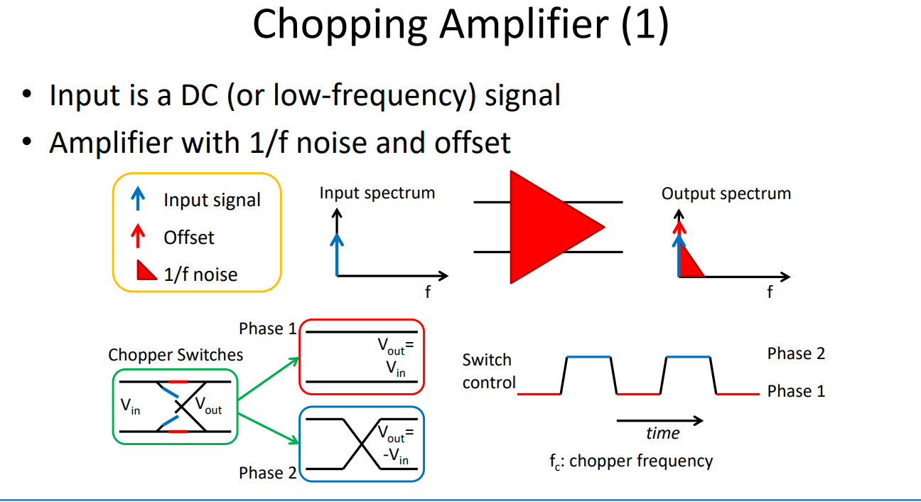
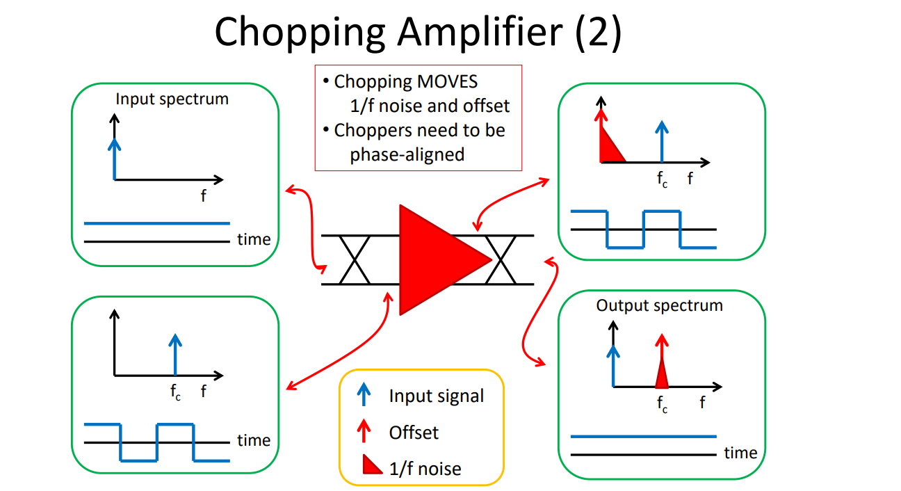
Chopper (electronics) - Wikipedia
*A chopper circuit is used to break up the input signal so that it can be processed as if it were an AC signal, then integrated back to a DC signal at the output. In this way, extremely small DC signals can be amplified.
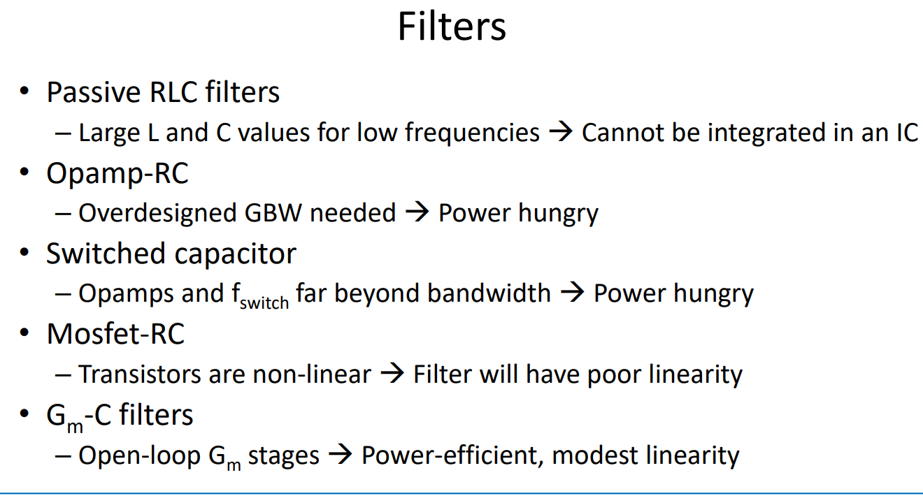
- Passive RLC for high
requires very large passive RLC values so cant be used on integrated circuits. - Opamp-RC
- OPAMP-Switched-capacitor
- Mosfet-RC
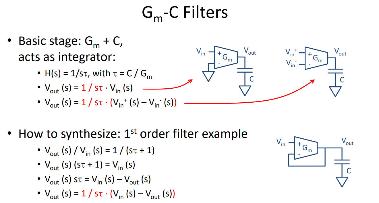
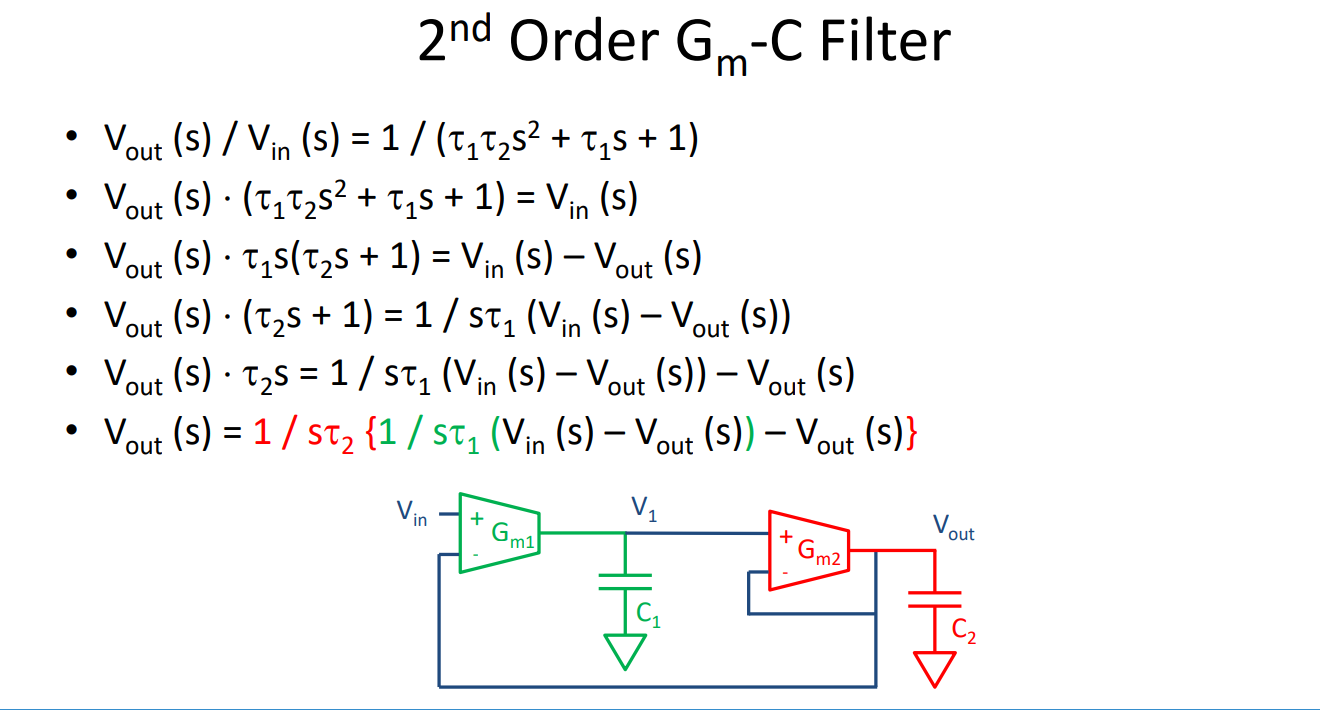
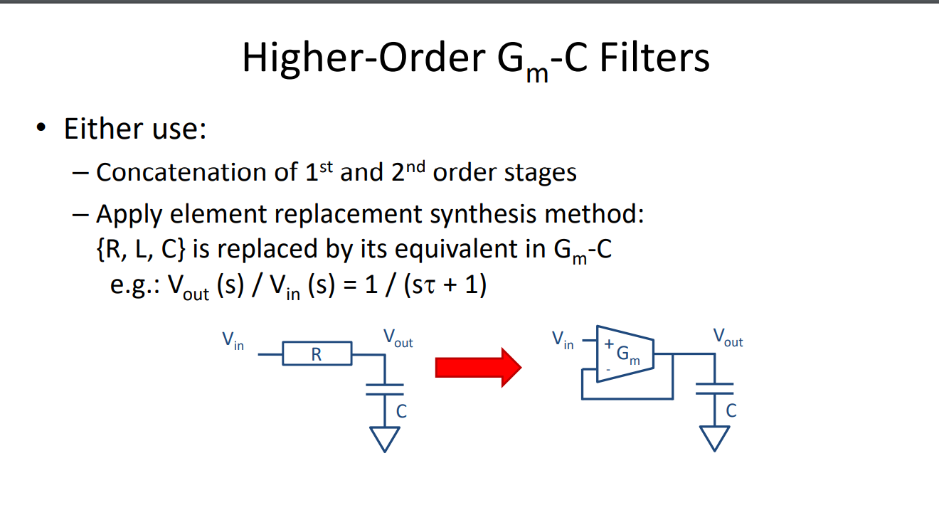
Digital. ADCs, and Layout
Topic: Data Converters
5XCC0-07 Digital, ADCs, and Layout.pdf
Formulas
Dynamic Power Consumption
Quantization noise (rms):
Total Power Consumption
Average Power from Simulation
Dynamic IR Drop
ADC Parameters
ADC Resolution / Dynamic Range
Nyquist Criterion
SAR ADC Voltage Step
Capacitor Array for SAR ADC
Parasitic Impact on Full-Scale Range
Sampling Noise
(single-ended)
(differential) Signal Power and SNR
Power Consumption of DAC
MIM Capacitor
Random Mismatch
Systematic Gradient Offset
Wire Resistance and Capacitance
Static IR Drop
Thermal noise
Acquisition of neural signals
5XCC0-05 Acquisition of neural signals.pdf
Formulas
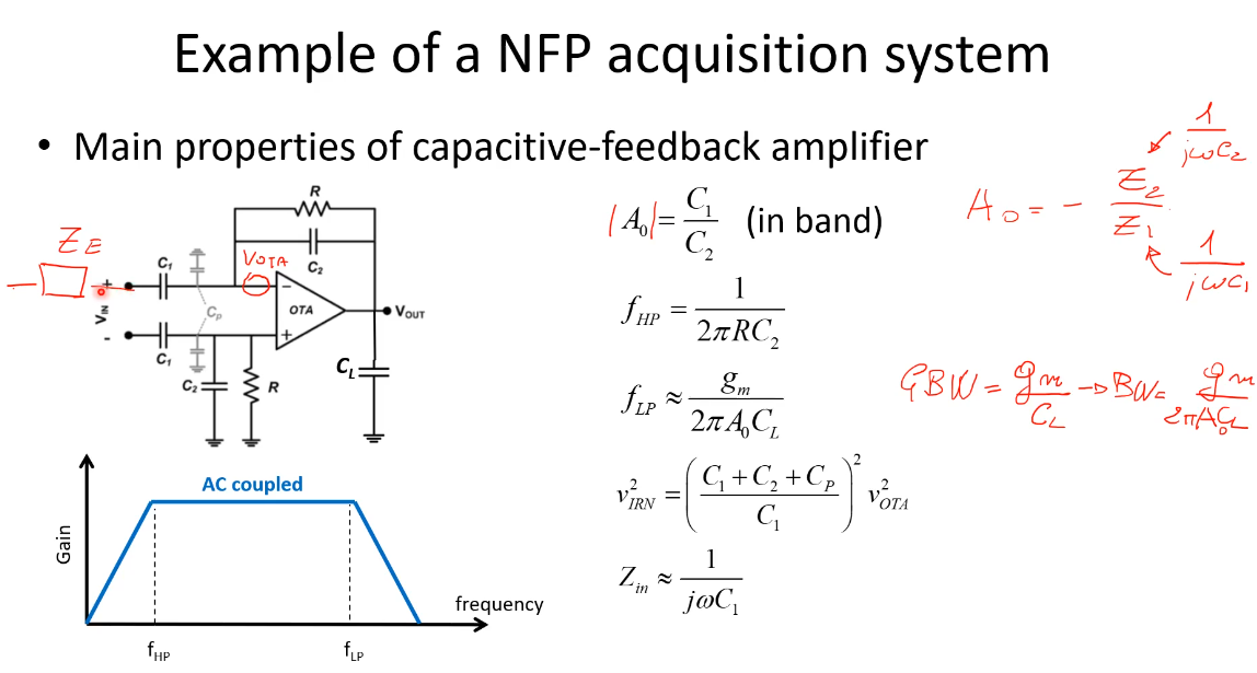
High-pass filter cutoff frequency (from AC coupling):
Amplifier Gain (capacitive feedback amplifier):
Low-pass cutoff frequency (in capacitive feedback):
Input-Referred Noise (IRN):
Input Impedance (for capacitive input):
Pseudo-Resistor Effective Resistance:
Noise corner shift due to increased bias current:
(not a formula, but remember that increasing bias shiftsto a higher frequency) Chopping Requirement:
Chopping frequencyChopping Duty Cycle Requirement:
Must be exactlyto avoid DC offset in modulated signal
Stimulation of neural tissues
5XCC0-06 Stimulation of neural tissues.pdf
Formulas
- Nernst Equation:
- Butler–Volmer Equation:
- Electrode Current Density:
- Overpotential:
- Safe Stimulation Limit (Shannon equation):
- Strength-Duration Relationship (Weiss Law):
- Charge:
- Charge Density per Phase:
- Charge Transfer Resistance (ideally):
for safe implanted electrodes - Power Dissipation:
- DC current avoidance (concept): ensure
over time to avoid electrolysis