Resit notes for Electronics II - 5ECC0
Oscillator Condition
Topic: Feedback and Stability
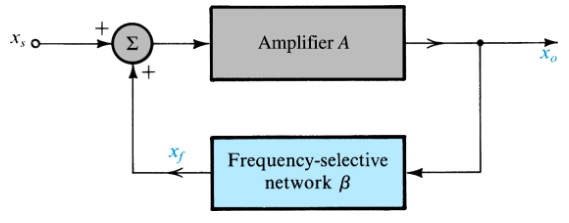
Open loop gain:
Barkhausen criteria for oscillation (necessary, != sufficient):
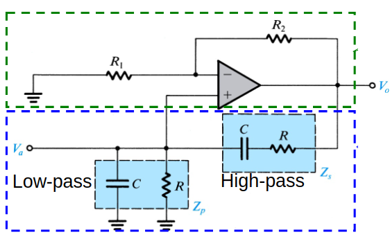
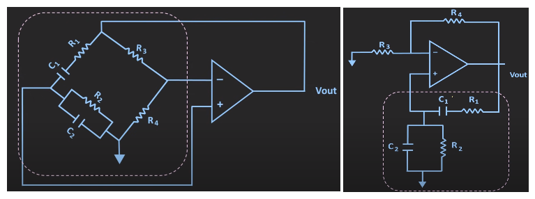
Barkhausen criteria:
- Zero phase at:
- = 1: stable
-
1: increasing
- < 1: decreasing
→ To stabilize:
Clipping (Electronics I - 5ECB0 > Limiters)
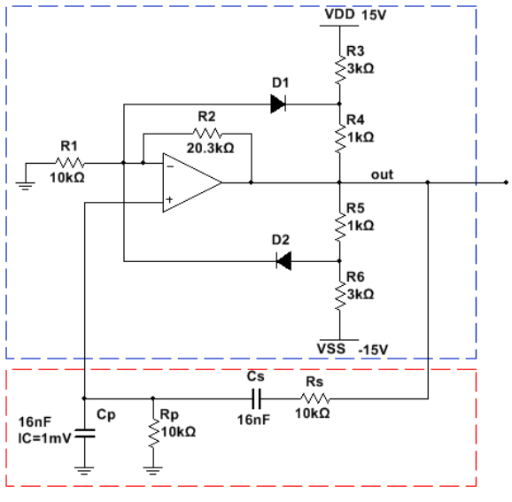
Phase Shift Oscillator
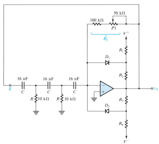
Implement
Quadrature Oscillator
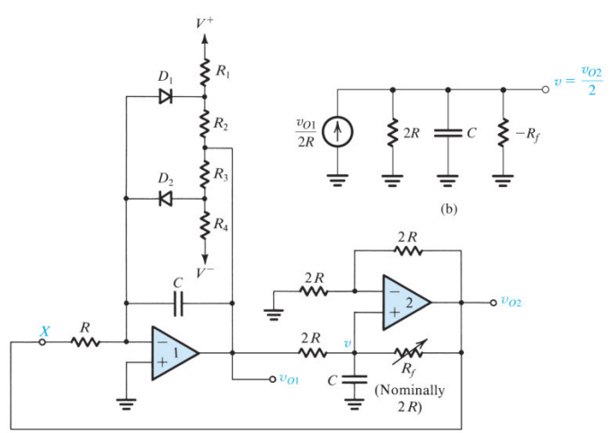
Similar to Phase shift oscillator, but implement phase shift
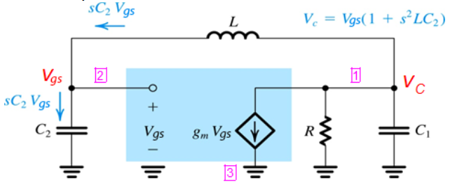
LC Oscillator
Difference:
- Complex poles and zeroes ??
- Better frequency selectivity
- Better roll off
- Osc freq more resilient to amplifier phase shift
- Better spectral purity
- Only applicable to HF and RF (as large inductance coils have large losses)
Analysis Method
Method 1: Cut the loop at point with infinite impedance (transistor gate) or controlled voltage source
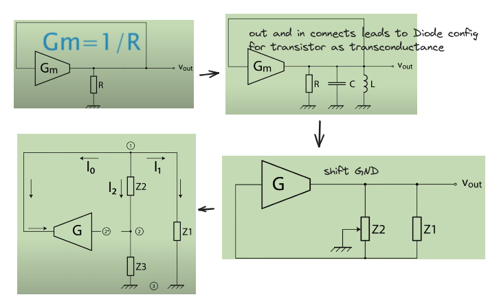
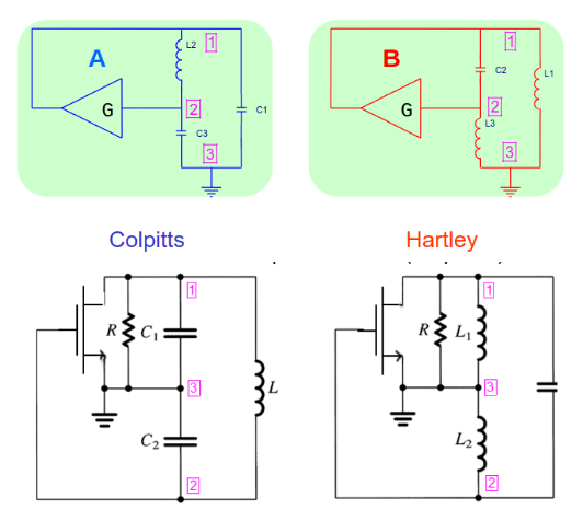
Method 2: KCL
Crystal Oscillator
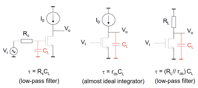
Capacitance
MOSFET (resit) - 5ECC0 > Common source
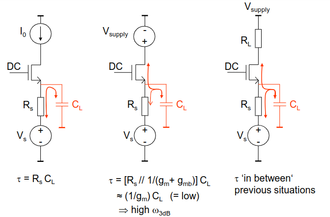
MOSFET (resit) - 5ECC0 > Common gate
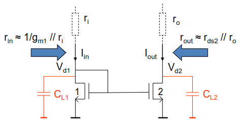
MOSFET (resit) - 5ECC0 > Current steering
Only
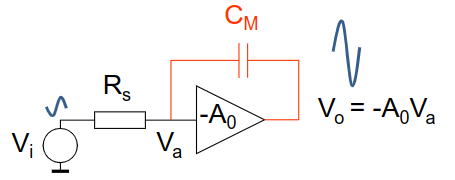
Miller effect
Large Signal Operation
Limitations:
- Output voltage/current saturation
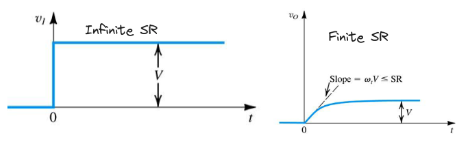
- Finite slew rate:
- Finite full power bandwidth:
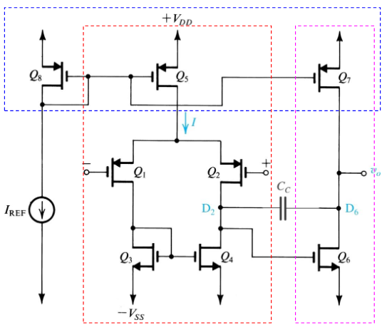
Two-stage CMOS Op-amp
Topic: Operational Amplifiers
First gain stage: Q1-5 (Differential Amplifier (resit) - 5ECC0 > Current mirror)
Second gain stage: Q6-7 (CS with active load current source)Frequency Response
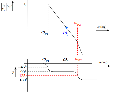
Topic: Transfer Functions and Frequency Response
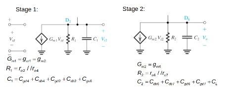
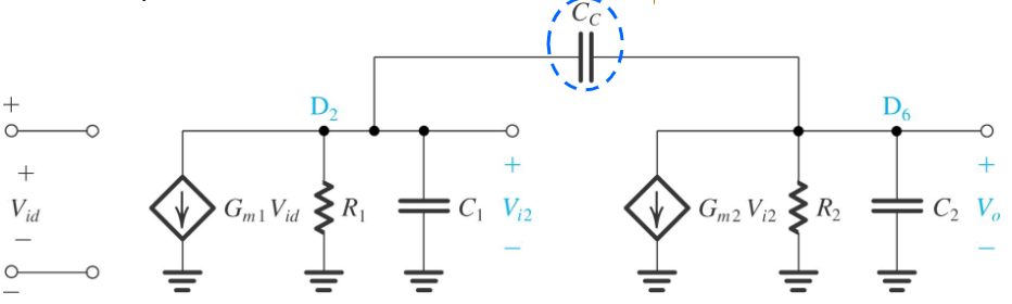
Without C between D2 and D6:
For: Phase > -
With C between D2 and D6
Intuition
Adding
also improves stability by switching to single stage amplifier (shorting Q6) at high frequencies Offset
Common-mode Range
Lower bound:
in saturation
Upper bound:
in saturation
Output Swing
Lower bound:
in saturation
Upper bound:in saturation
Small-signal Gain
1st stage:
Phase Margin
Topic: Feedback and Stability
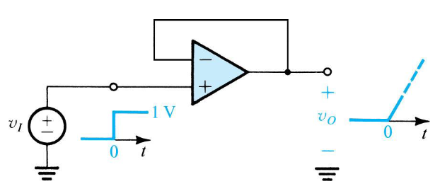
Slew Rate
Note
Finite SR cause large differential voltage → turn off one side of differential pair current
Common Mode Rejection Ratio
Only first stage Differential Amplifier (resit) - 5ECC0 > Current mirror
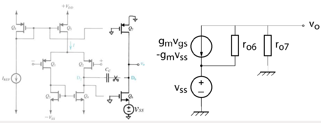
Power Supply Rejection Ratio
( don’t affect circuit function)
Link to original
Output Stage
Switch Mode
Class D: very high efficiency (90-95%)
Linear Mode
Class A: current flow in whole period → low efficiency (max 25%, ~10-20%)
Class B: current flow in half period → high efficiency (max
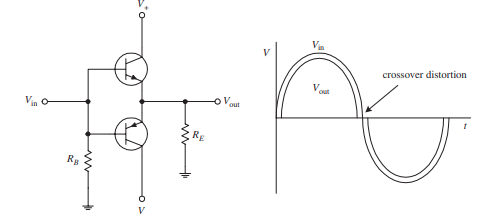
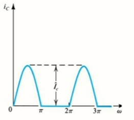
Class A/B: both are on for some time → a bit lower efficiency than class B but no crossover distortion by introducing voltage difference
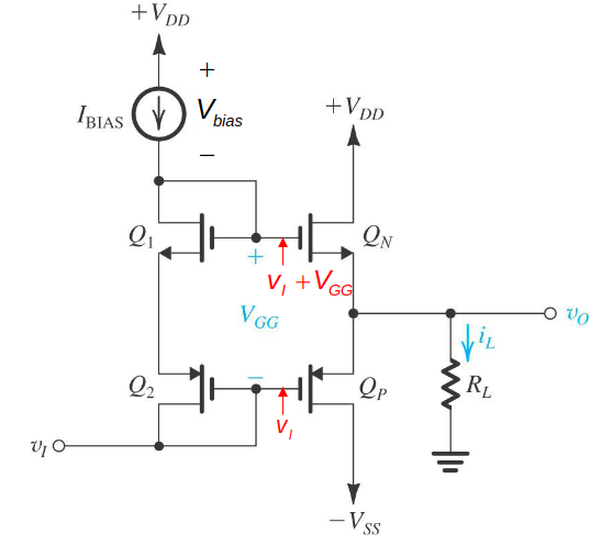
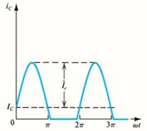
Matching PMOS and NMOS current:
Output voltage swing:
Upper bound:
Lower bound:
→ Output voltage swing is reduced
→ Common source with negative feedback to reduce output resistance
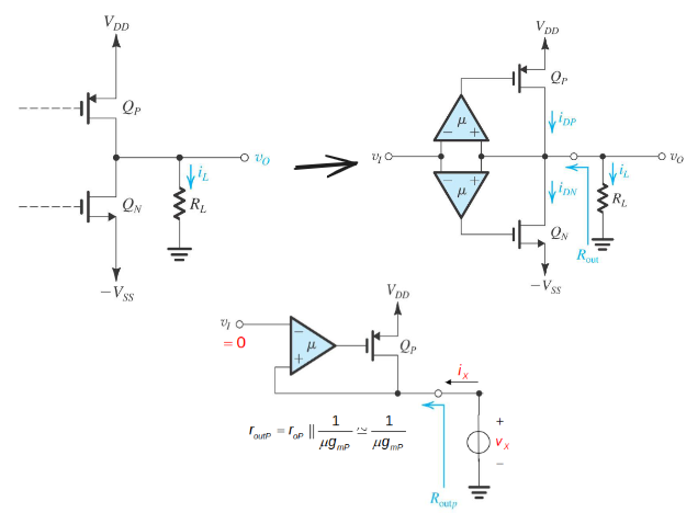
Output voltage swing:
Output resistance:
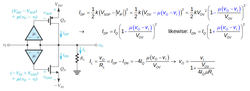
Error:
Negative feedback → high frequency issues with Barkhausen criteria
Motivation:
<% tp.file.cursor(1) %>
Definition:
<% tp.file.cursor(2) %>
Properties:
<% tp.file.cursor(3) %>
Related concepts:
<% tp.file.cursor(4) %>