Resit notes for Electronics II - 5ECC0
- Topics: MOSFET · Transistor Amplifiers · Digital Logic
MOSFET/MOST
Topic: MOSFET
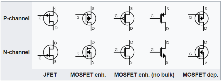
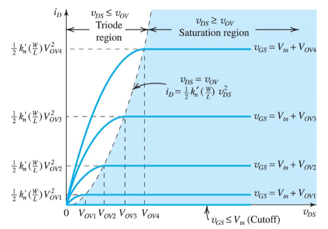
Deep Triode (small
Conductance:
: mobility
: oxide capacitance
: process transconductance parameter
W, L: width, length of MOST
: overdrive voltage
→ Voltage controlled resistor with small
Tapered Channel
Triode:
Saturation:
Body effect:
Amplifier
Topic: Transistor Amplifiers
Transconductance:
Channel length modulation:
@
(early voltage):
→ Equivalent output resistance:
Gain with channel-length modulation:
Hybrid-
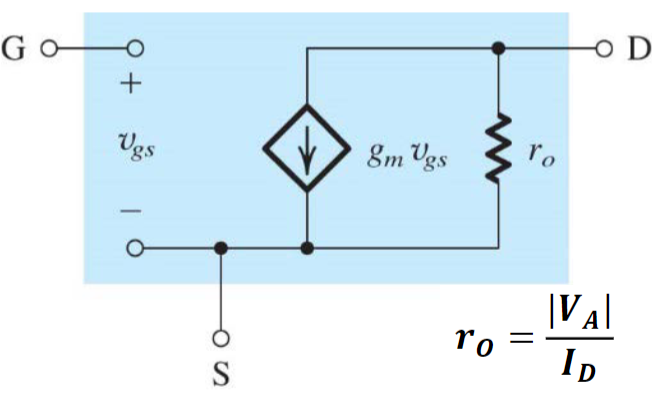
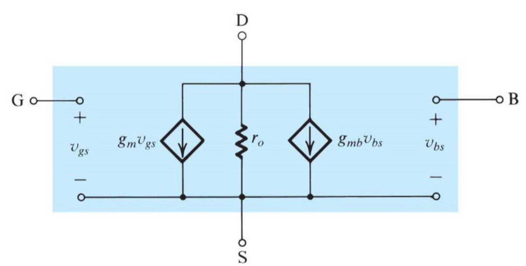
T model: modified version of Hybrid-
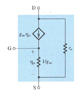
Body effect:
Maximum
Configurations
Topic: Transistor Amplifiers
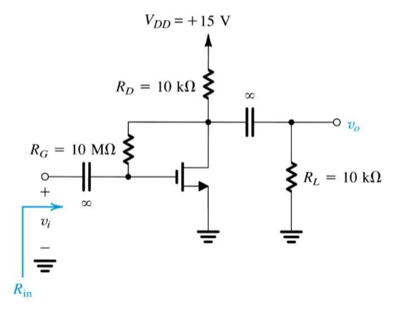
Diode connected
Equivalent diode with resistance:
Common Source
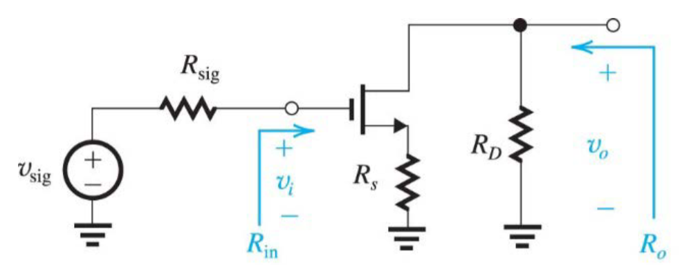
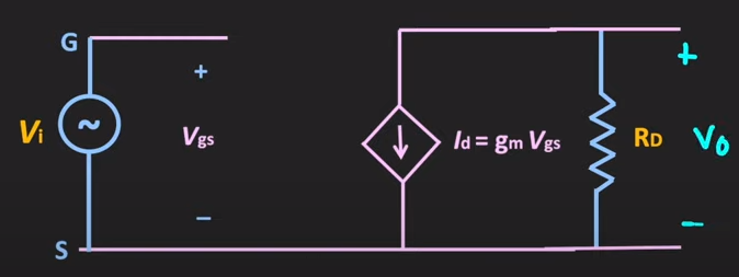
Input resistance:
Gain:
Add
Ideal gain:
- Very high/inf
, high - High V gain
- Add CD for low
Common Gate
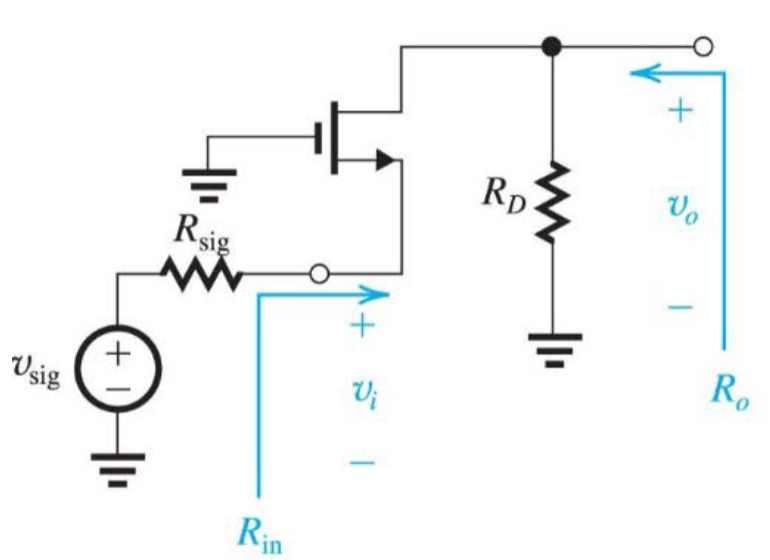
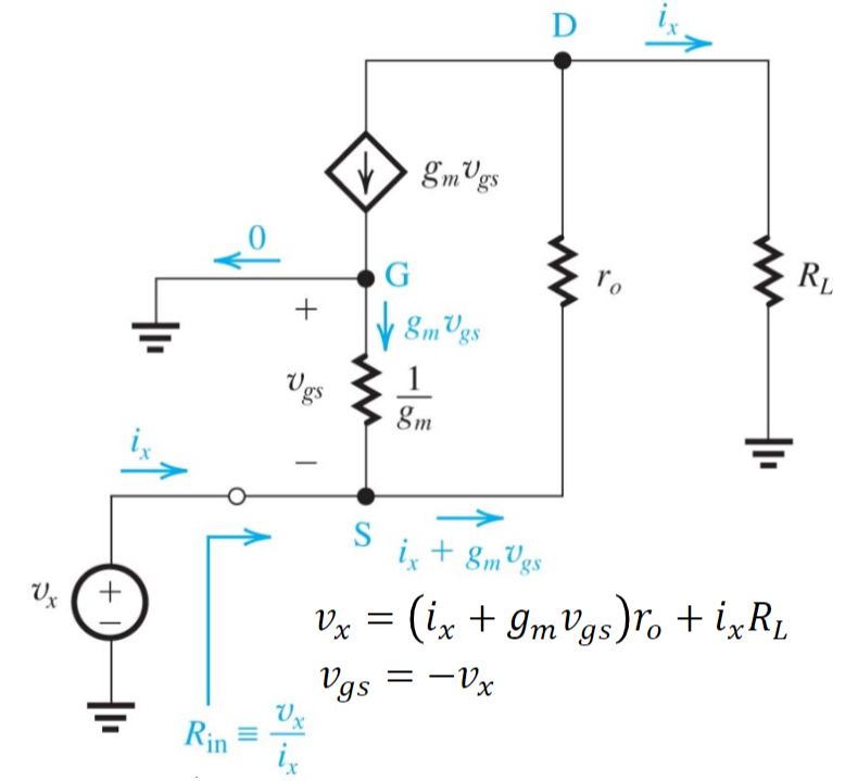
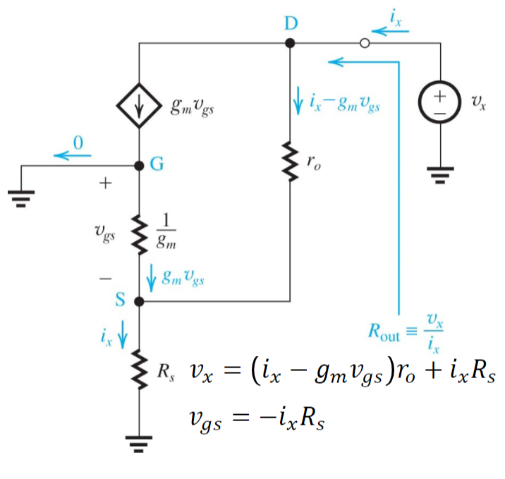
Ideal:
Real:
Gain:
- Low, controllable
impedance matching with low impedance sources (cables…) >< Input severely attenuated - High
cascode amp
Common Drain (source follower)
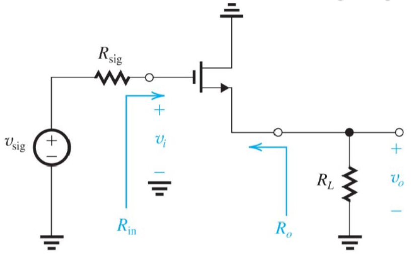
- Very high, inf
, low, controllable - ~1 gain
- Last stage for low
Current Mirror (resit) - 5ECC0
Resit notes for Electronics II - 5ECC0
- Topics: Current Mirrors
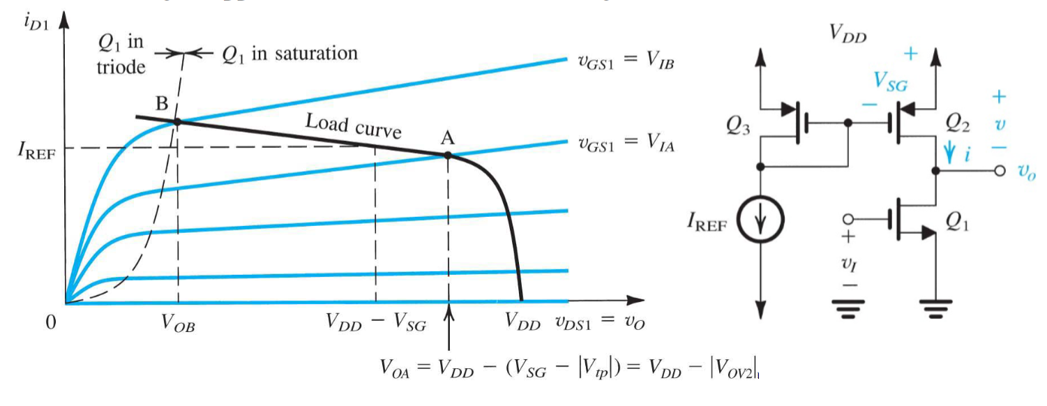
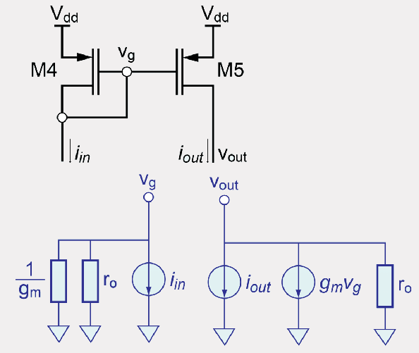
Current Steering
Load curve: I-V of Q2 (
)
Link to original
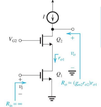
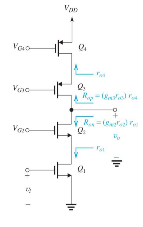
Cascode (Common gate + Common source)
Active loading: replace load resistance with current source
Differential Amplifier (resit) - 5ECC0
Differential Amplifier (resit) - 5ECC0
Resit notes for Electronics II - 5ECC0
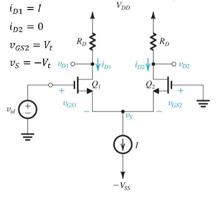
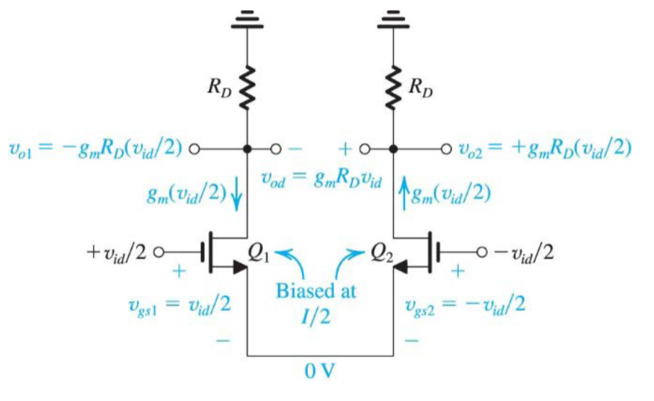
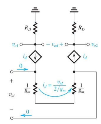
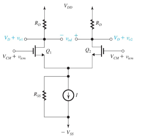
- Topics: Current Mirrors · Differential Amplifiers
Resistor
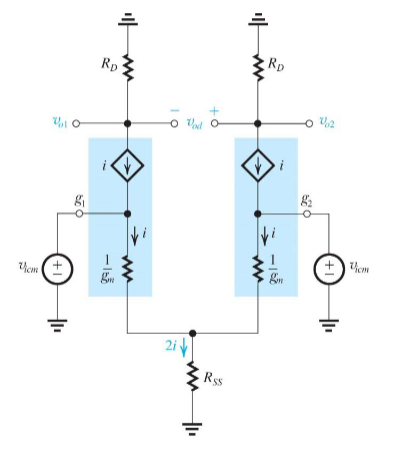
Common mode:
Differential mode:Virtual GND is established at D → no bypass C to GND in SSA
One side switched off:
→ Current source:→ cascode CMRR:
Current Mirror
Topic: Current Mirrors
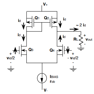
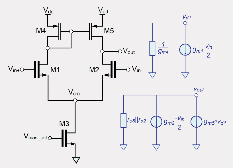
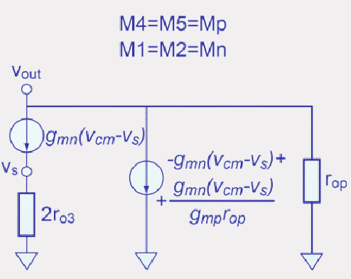
Active load:
Differential gain:
Common mode gain:
Current Mirror (resit) - 5ECC0
Link to original
Inverter
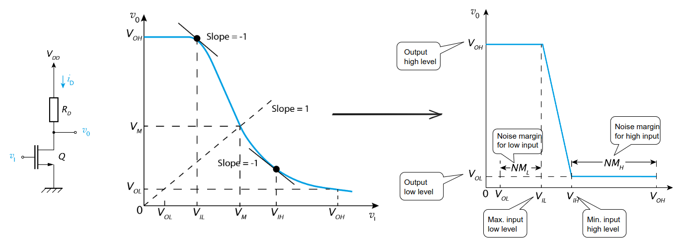
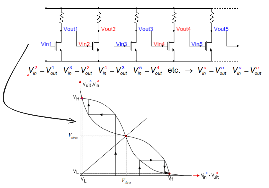
mid/trip point
Load line analysis
Dynamic power dissipation
Source input energy:
Dissipated power when charging:
When discharging:
Power dissipated:
Propagation delay:
Figure of Merit (FoM) to compare technology:
- Power-Delay Product PDP :=
( might be cancelled out at maximum frequency) - Energy-Delay Product EDP :=
Complemetary inverter
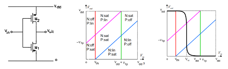
Triode:
Saturation:
When both N and P in saturation (ignoring channel-length modulation):
For matched transistor
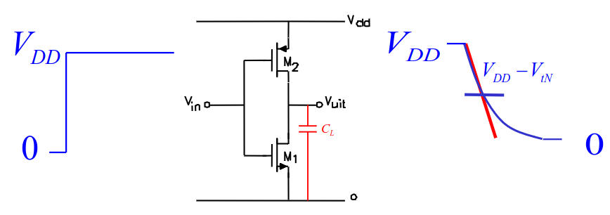
Static power << Dynamic power (if input transition >>)
Propagation delay
Similar for
For matched transistor:
- For
- For
CMOS logic
Topic: Digital Logic
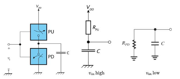
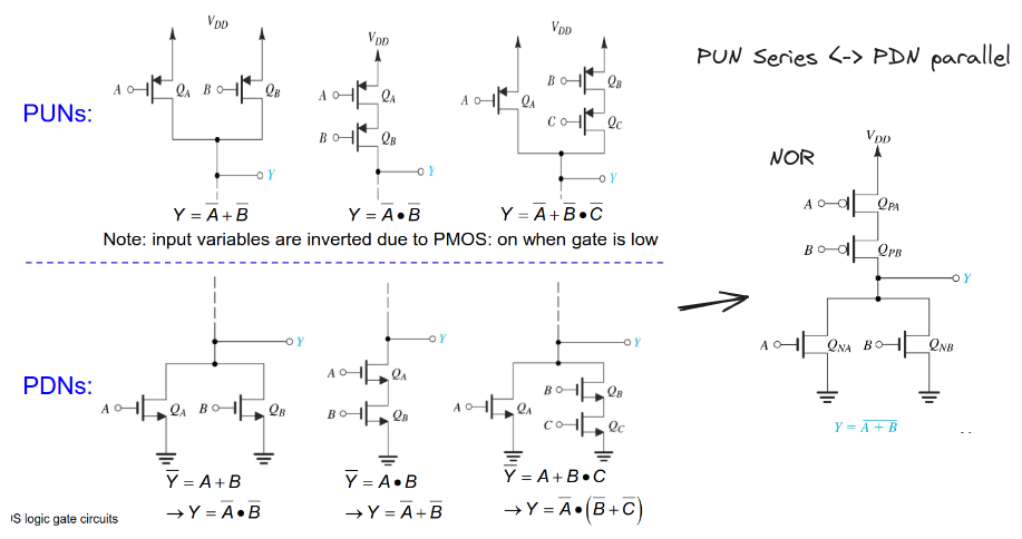
Transistor sizing:
- minimize area → minimum length of tech
- ensure min discharge current ~ 1 mos →
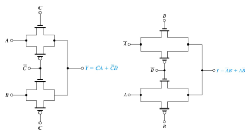
Transmission gate
Can be used as:
- Controllable switch
- Combine with capacitor to mimic resistor
- Building block in transistor-transistor logic (TTL)
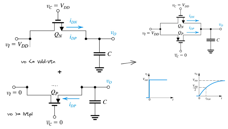
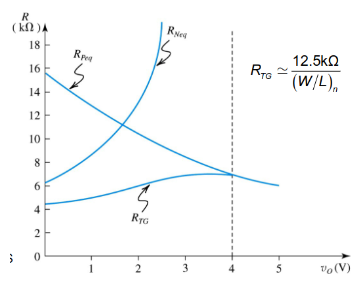
Resistor
- Saturated mode:
- Off mode:
- Saturated mode:
- Triode mode:
TTL building block
Memory circuit
Topic: Digital Logic
- Static: only need supply
- Dynamic: based on charge conservation → need refresh
Requirements: - 2 stable states
- Controllable
- Observable
2 stable states
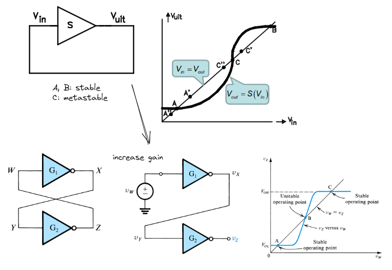 Stable:
Metastable:
For a continuous static transfer characteristic
between two stable points there will always be a metastable point
Every (practical) loop with a metastable point has (at least)
two stable points
out inV S V
(‘saturation’, for example due to limited supply voltage)
A circuit with exactly two stable states is called ‘bi-stable’
A bi-stable circuit will need an amplifier, that for a certain voltage range
has >a (positive) small-signal voltage gain 1
Controllable
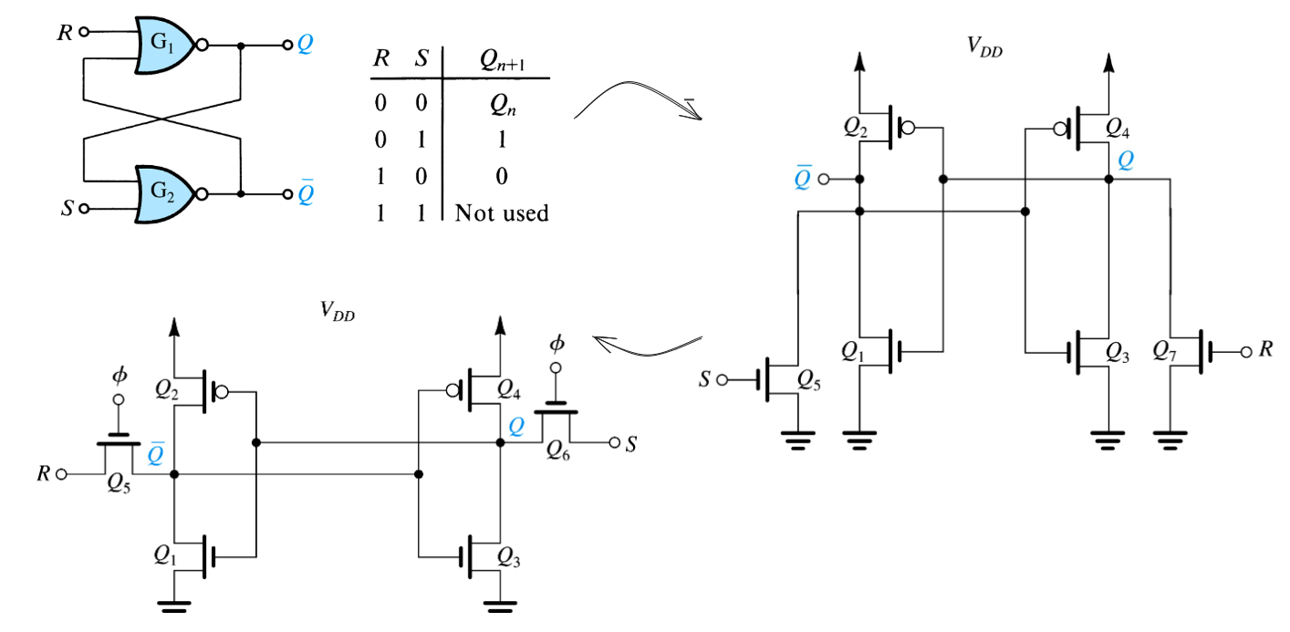
Static
read write operation
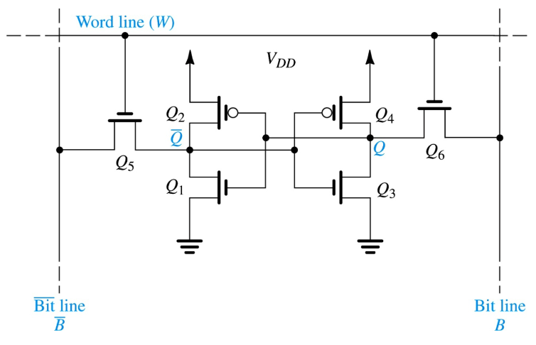
Read:
Note
Non destructive → Need to design so that
Bit lines are precharged
Write:
Suppose writing 0
→ wait for Q to switch to 0
Dynamic
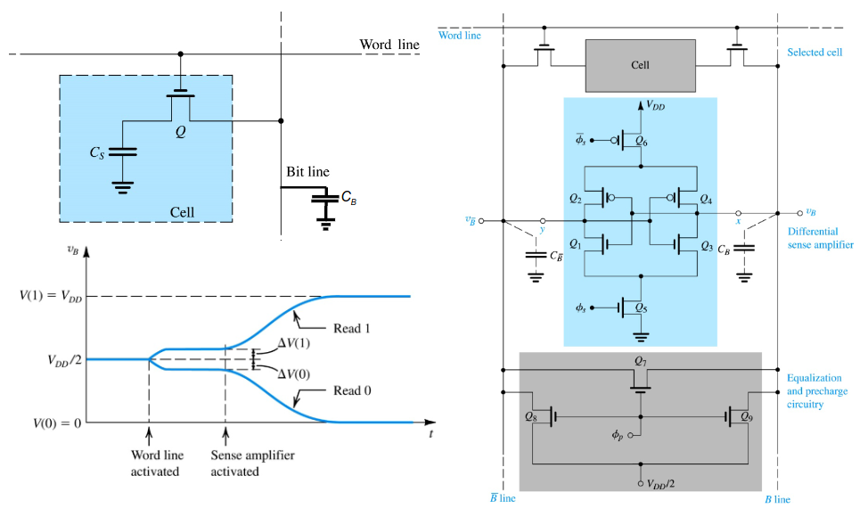
Need to maintain precharge voltage of bit lines every cycle
Read:
Write:
- Bit lines are precharged → sense amp in metastable state
and exchange charges: - Unbalance
- Sense amplifier raise to stable states