Resit notes for Electronics II - 5ECC0
Op-amp
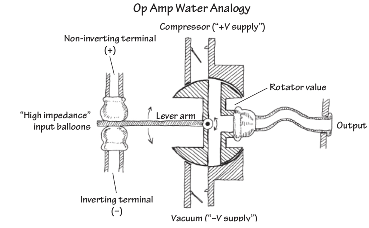
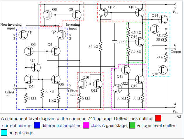
Negative feedback:
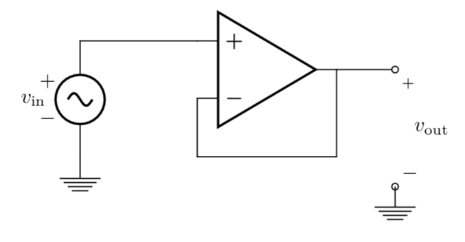
Buffer
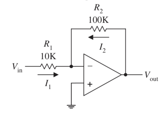
Inverting amplifier (G = -R2/R1)
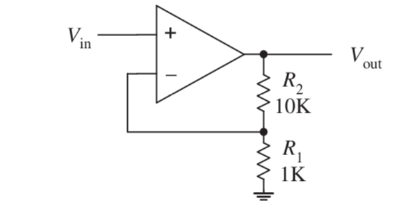
Noninverting amplifier ( G = (R1+R2)/R1 )
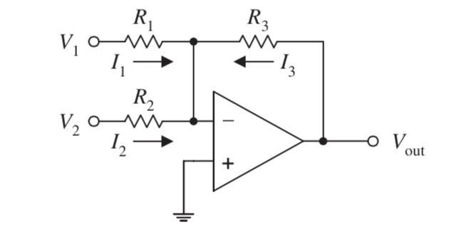
(-) Summing amplifier ( Vout = -(R3/R1V1 + R3/R2V2) )
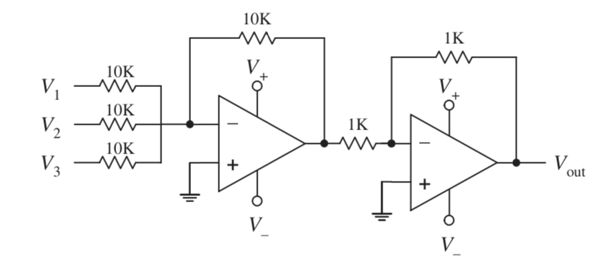
(-) Summing amplifier + Inverting amplifier → (+) Summing amplifier
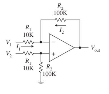
Inv + Non-inv amp → Differential amplifier (Vout = V2*(R1 + R2)/R1 - V1R2/R1 = R2/R1(V1 - V2))
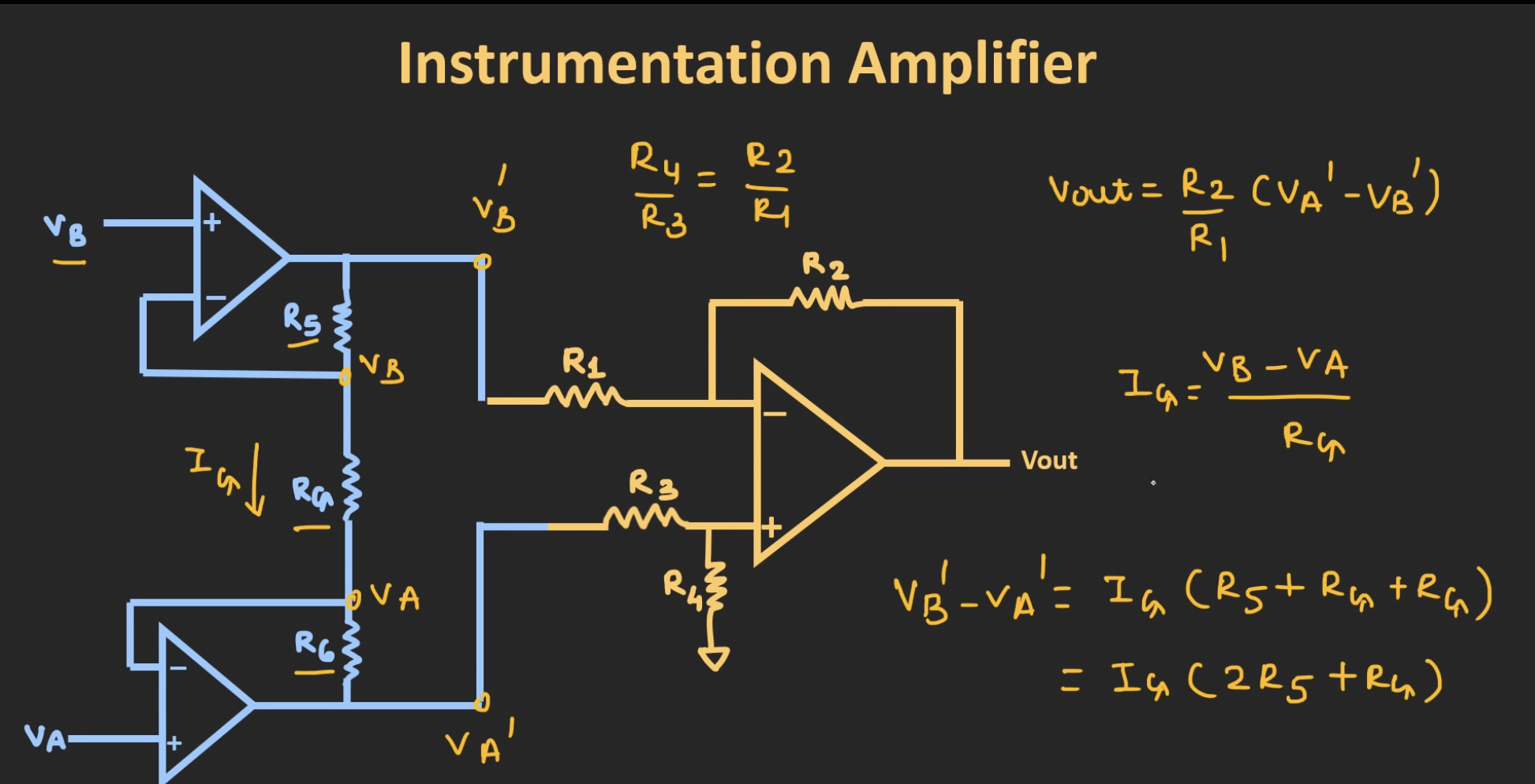
Instrumentation amplifier (Differential amplifier + Noninverting amplifier → zero impedance to avoid CMRR from mismatched resistor) + Rg for adjusting gain
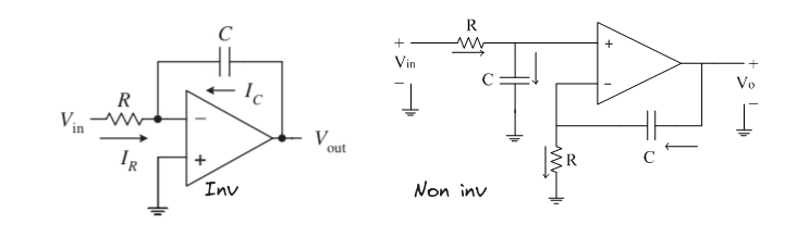
(Miller) Integrator (Vout = -1/(RC)F(Vin))
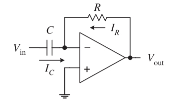
(Inv) Differentiator (Vout = -RCVin’)
Non-inv Differentiator
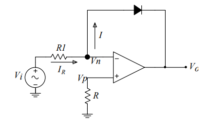
Logarithmic amplifier
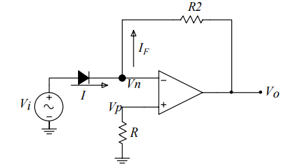
Antilog amp
Positive Feedback
Topic: Oscillators and Waveform Generators
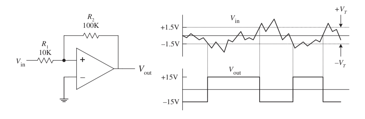
Schmitt trigger (hysteresis effect Vth = +- Vs*R1/R2)
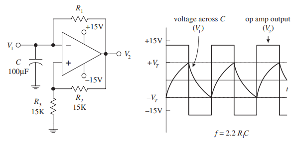
Square wave (Astable multivibrator, T = 2R1ln(1+2R3/R2))
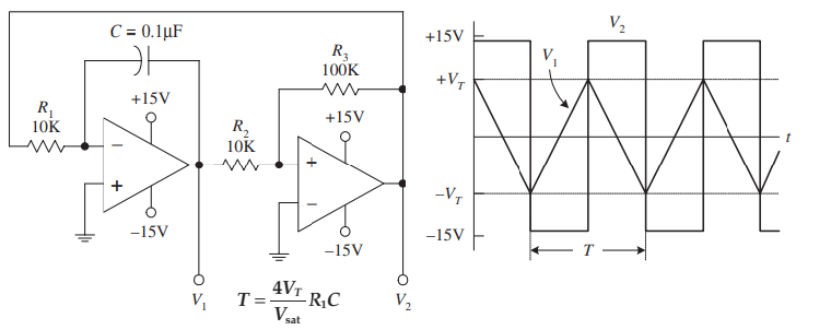
Triangle + Square wave
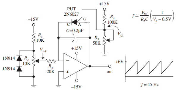
Sawtooth generator (PUT with ~0.5 Vdrop set threshold to quickly discharge C)
Comparator
Op-amp but output circuitry is a transistor
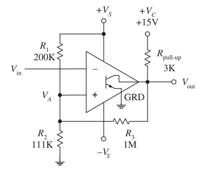
Inverting comparator with hysteresis
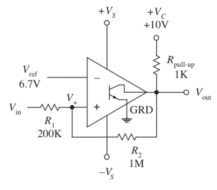
Noninverting comparator with hysteresis
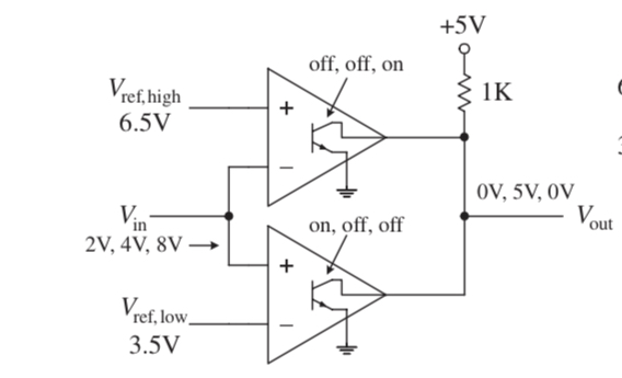
Window comparator
Miscellaneous
59E321E0-0F30-4754-9AAD-AB36FA177BA1.jpeg (not included in the repository)
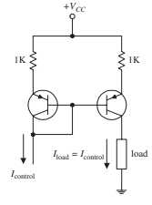
316E130F-F2C2-495E-9287-369450D8FE86.jpeg: V to I converter (not included in the repository)
V to I converter
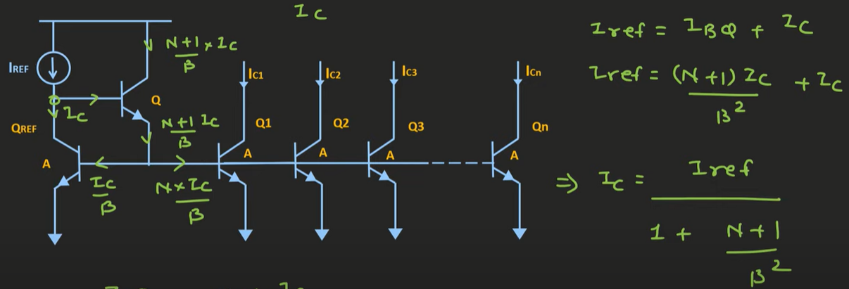
Hold V in C (I_in ~ 0)
Peak detector
- Buffer (eliminate diode Vdrop) → Superdiode
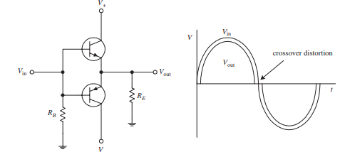
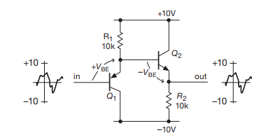
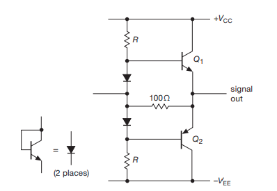
Push-pull + Op-amp → Eliminate crossover
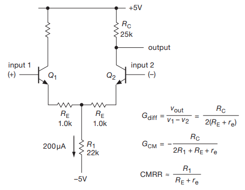
Smoke detector (use diode as LED and photodiode
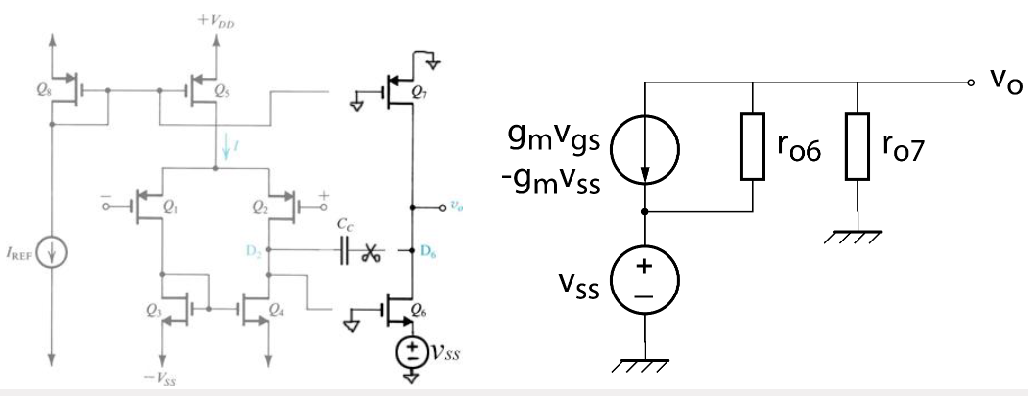
Two-stage CMOS Op-amp
Topic: Operational Amplifiers
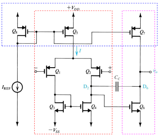
First gain stage: Q1-5 (Differential Amplifier (resit) - 5ECC0 > Current mirror)
Second gain stage: Q6-7 (CS with active load current source)
Frequency Response
Topic: Transfer Functions and Frequency Response
Without C between D2 and D6:
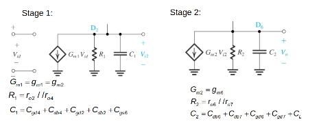
For
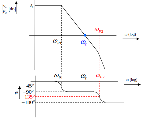
With C between D2 and D6
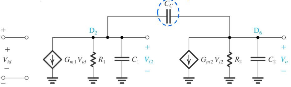
Intuition
Adding
also improves stability by switching to single stage amplifier (shorting Q6) at high frequencies
Offset
Common-mode Range
Lower bound:
Upper bound:
Output Swing
Lower bound:
Upper bound:
Small-signal Gain
1st stage:
Phase Margin
Topic: Feedback and Stability
Slew Rate
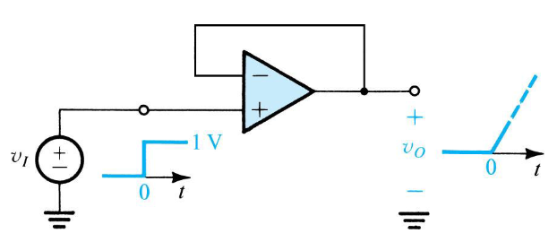
Note
Finite SR cause large differential voltage → turn off one side of differential pair current
Common Mode Rejection Ratio
Only first stage Differential Amplifier (resit) - 5ECC0 > Current mirror
Power Supply Rejection Ratio